AFM-based Nano-probing
|
Technical Concept |
|
Atomic force microscopy (AFM) based nanoprobers are one of the state-of-the-art solutions to achieve precise fault isolation on nano-scale with its high spatial resolution. |
How to achieve precise fault isolation on nano-scale is a challenge and urgent task with the fast-paced development of miniaturization technology. With its high spatial resolution, atomic force microscopy (AFM) based nanoprobers are one of state-of-the-art solutions for such a purpose.
Different from SEM-based nanoprobers, the loading force of probers for the AFM-based nanoprober can be precisely controlled via a feedback system and most impressively, electron accumulation effect which may cause electrical damage is negligible during probing. Nowadays, this technology provides special resolving power down to 10 nm.
The AFM-based nanoprober also provides many AFM-related functions, such as pico-current imaging and scanning capacitance microscopy (SCM). These functions strengthen the inspection power for failure analysis and therefore such technology is promising in the application of developing advanced semiconductor devices.
|
Specifications/capability |
- Measuring technology node can be down to 10 nm
- 8 prober
- W tips/apex diameter: 15-35 nm
- Low contact resistance < 30 ohm
- Target area < 200 um
- Low thermal drift ~ 1 nm
- Nitrogen purged environmental enclosure to prevent oxidation
|
Features |
- High-spatial resolution ~ 10 nm
- No electron beam effect
- Contact/tapping modes imaging
- Force feedback control
- Pico-current sensitivity ~ 5 pA
- Scanning capacitance microscopy function
|
Equipment |
 |
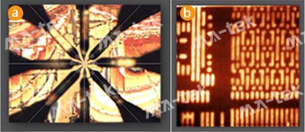 |
(a) OM image of 8 probes ; (b) Tapping mode AFM image
With the help of pico-current, the current on a specific path can be measured.
 |
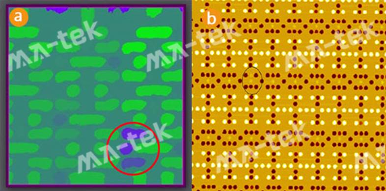
(a) OM image of ROI ; (b) AFM image of ROI ; (c) Pico-current image
With the help of pico-current and SCM, failure locations can be identified for further FA analysis. Areas marked by a red circuit and a black ellipse exhibit the failure locations. Images are provided by Multiprobe, DCG.
 |
(a) Pico-current ; (b) SCM
|
Contact |
|||||
|