
Silicon Photonics (SiPh) Analysis & Testing Service
As the demand for AI compute skyrockets, people have turned to photonics to address the data transmission bottleneck.
In response, MA-tek offers the “SiPh Wafer and Chip Optoelectronics Analysis and Testing Platform”, bridging optics andsemiconductor materials analysis to overcome yield rate issues with Co-Packaged Optics and expedite productcommercialization.
Everything from Fault Localization to Root Cause Analysis
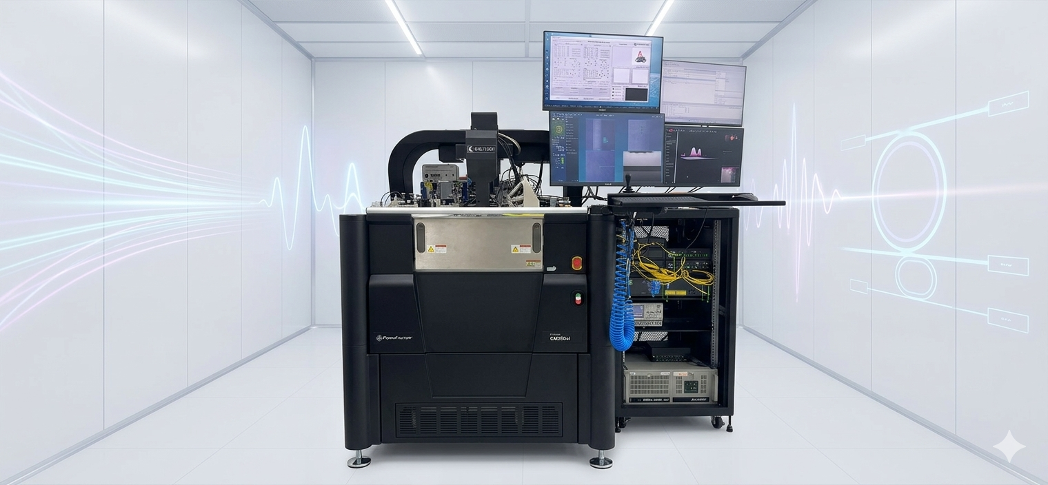
- Precise Fault Localization: Identify SiPh insertion loss, localized optical leaks, device defects, and other optoelectronic characteristics through Optical-to-Optical (O-O) and Electrical-to-Optical (E-O) testing
- Materials Analysis: Examine nanoscale waveguide sidewall roughness, material composition, and defects through ultra-high resolution Scanning Electron Microscopy (SEM), Focused Ion Beams (FIB), Transmission Electron Microscopy (TEM), and Scanning Transmission Electron Microscopy (STEM)
- Dopant Analysis: Measure dopant concentrations and depth profiles in germanium, waveguides, Photonics Integrated Circuits (PICs), and III-V semiconductor materials with Secondary Ion Mass
Our SiPh Analysis and Testing One-Stop Shop
Integrating full-spectrum near-infrared optical imaging and nanoscale photonic alignment systems, we provide a comprehensive, automated platform for all your optoelectronic characterization and failure analysis needs.
| Test Categories | Applications | Key Metrics | Benefits and Advantages |
|---|---|---|---|
| Basic Optoelectronics and Functionality Testing |
Chip-Level/Device-Level • Basic Optoelectronics Characterization |
|
|
| Passive Testing |
Optical Fibers and Interfaces
|
Easy Package Alignment: Measure optical conversion efficiency and improve packaging processes |
|
|
Signal Transmission
|
Yield Rate Optimization: Accurately identify waveguide defects and optical leaks to quickly refine chip manufacturing |
||
| Active Testing |
Opto-Electronic Converters
|
Testing dynamic and static characteristics of PIC active components |
Efficient Performance Testing: Ensure 200+ G/lane data transmission and conversion efficiency |
Contact
Contact Window
Material Analysis Technical Consultation (MA)



