Material Analysis
The composition and uniformity of packaging materials directly affect the electrical performance, mechanical strength, and long-term reliability of components. Through high-resolution material analysis technology, it is possible to identify the composition and analyze the structure of each layer of materials in the packaging, accurately grasping material characteristics and process quality.
The analysis scope covers packaging resins, solder, metal layers, dielectric materials, die attach, and surface coatings, which can confirm material formulations, elemental distributions, sources of contaminants, and abnormal components. Through cross-sectional and localized analysis methods, it can effectively assess potential risks caused by material degradation, interfacial reactions, metal diffusion, or process deviations.
Packaging material and composition analysis can not only be used for failure analysis but is also often applied in new material introduction verification, process comparison, supply chain material consistency assessment, and reliability improvement, assisting customers in establishing a stable and traceable quality foundation before mass production and throughout the product lifecycle.
SIMS Applications
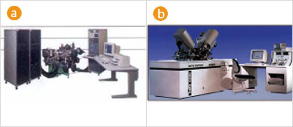
(b)ATOMIKA sims 4500; High Depth Resolution, Ultra-Shallow Junction
- Ultra-shallow junction analysis
- Very thin layer (tens angstrom) analysis
- Doping profile/Depth profile
- Back side Cu Diffusion
- Contamination verification
- Excellent detection limit (ppm to ppb)
- Can detect all elements and isotopes, including hydrogen
- Excellent depth resolution, 1nm is possible
- Quantification by standard reference
- Insulator can be measured
-
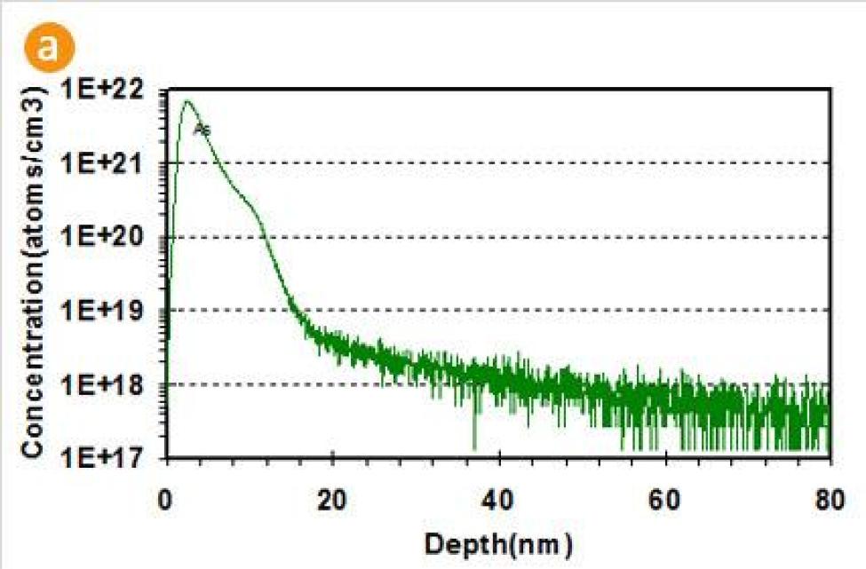 (a)Ultra Shallow Junction
 -
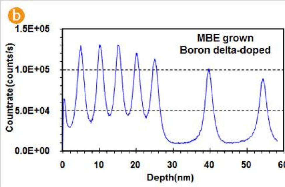 (b) High depth resolution
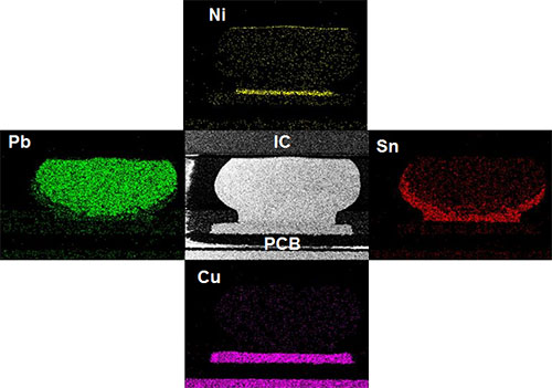
SEM/EDX Mapping Analysis