CP Ion Grinding
Ion Milling, also known asCross-Section Polishing(CP)is a sample preparation technique that uses high-energy ion beams to bombard the surface of the sample to remove material and form a smooth cross-section. In the process of semiconductor material analysis and failure analysis, in order to observe the microstructure inside the chip or package, such as multilayer metal wiring, dielectric layers, solder joint structures, or material interfaces, it is usually necessary to produce high-quality cross-sections of the samples. However, if only usingMechanical cutting or grindingstructural damage due to stress, plastic deformation, or material pulling, resulting in subsequentScanning Electron Microscope (SEM)The quality of observation is affected.
Ion milling technology throughHigh-energy argon ion beambombard the surface of the sample, allowing the material to be removed layer by layer, enabling the preparation oflow stress, low damage and highly smooth cross-sectionTherefore, it is widely used in semiconductor, electronic packaging, materials science, and optoelectronic component analysis.
Ion grinding systems typically useInductively coupled RF source or microwave sourceGenerate plasma during the operation of the system:
-
Argon (Ar) is introduced into the plasma chamber.
-
High-energy electrons collide with argon atoms to produce a large amount ofpositive argon ion (Ar⁺)。
-
The electrode system accelerates these argon ions to form a high-energy ion beam.
-
The ion beam bombards the sample surface, gradually removing the material.
Through precise controlIon energy, incident angle, and processing timecan prepare flat and undamaged cross-sections, and after grinding, use againOptical microscope (OM) or scanning electron microscope (SEM)Conduct observation and analysis.
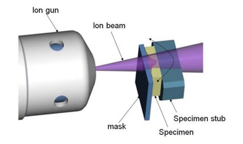
Cross-section Milling
In order to observe and analyze the internal structure of the sample, it is necessary to fully reveal the internal structure of the sample. If only cutting and mechanical grinding are used, deformation or damage often occurs due to material stress, making it difficult for SEM to obtain ideal images.Ion Beam Bombardment Processingcan prepare cross-sections with low stress and high flatness, allowing SEM to clearly observe the internal structure of the sample.
-
semiconductor multilayer metal structure
-
dielectric layer thickness
-
solder joint interface
-
Material interface defects
-
Foreign objects or contaminants
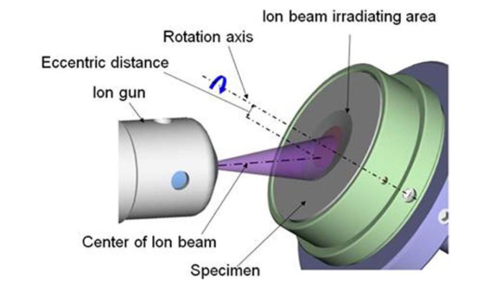
Flat Milling
In SEM surface observation and analysis, it is usually necessary toLarge area and flat sample surface,Flat milling uniformly removes the surface material of the sample through an ion beam, commonly used forSurface analysis or post-processing after mechanical grinding。
-
Remove the damage layer caused by mechanical grinding.
-
Flatten the sample surface
-
Provide a larger observation area
-
Improve SEM image quality
MA-tek has completeIntegration capabilities of ion milling and electron microscopic analysiscan provide high-quality sample preparation and precise material analysis.
- High-quality cross-section preparation capability:Can prepare low-stress, low-damage, and high-flatness sample cross-sections.
- Applicable to various material systems:Applicable to semiconductor, PCB, packaging materials, LED, and metal materials analysis.
- Large area sample processing capability:Can prepare large area observation regions, suitable for structural analysis and process diagnosis.
- Cross-technology integration analysis capabilities:can be combinedSEM, EDS, EBSD, FIB, TEMand analysis techniques, providing complete material analysis solutions.
-
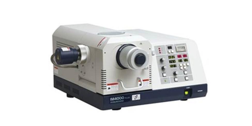
Image | Ion Milling System ArBlade 4000
ArBlade 4000 ion milling system provides stable ion beam processing capabilities, suitable for high-quality cross-section preparation of semiconductor and electronic materials.
-
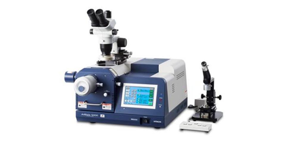
Image | Ion Milling System ArBlade 5000
The ArBlade 5000 ion milling system has a higher precision ion beam control capability, allowing for the preparation of large area and low damage sample cross-sections.
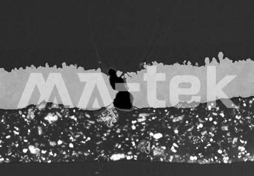
FFC abnormal sample analysis
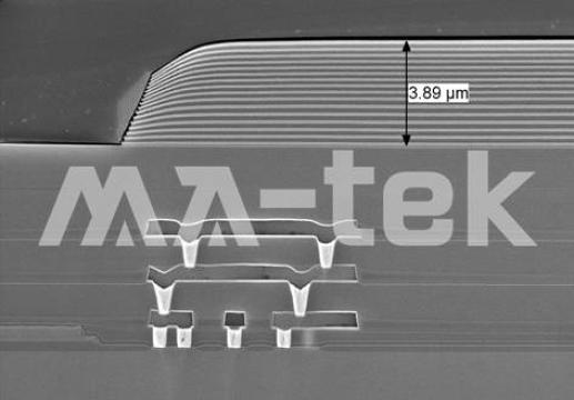
Analysis of the cross-section of photosensitive devices (CCD / CMOS)
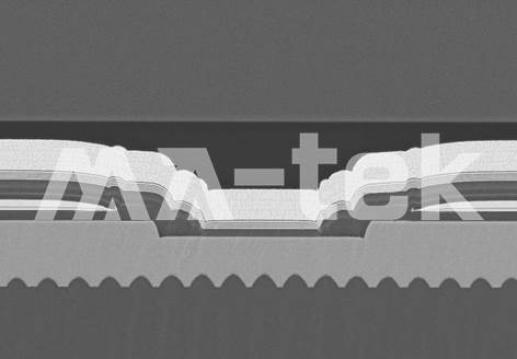
LED sapphire substrate material analysis

Copper grain microstructure observation