CMOS image sensor
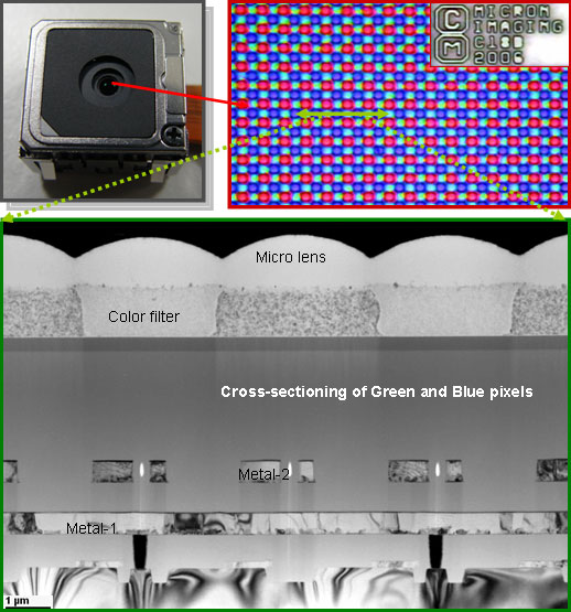
Common issues in the CMOS image sensor manufacturing process include dark current, hot pixels/dead pixels, metal contamination, thin film defects, microlens misalignment, and optical structure abnormalities. These defects can affect image quality, light sensitivity, and component reliability, thus requiring precise localization and failure mechanism analysis through high-resolution material analysis and structural inspection techniques.
MA-tek integrates material analysis (MA), surface analysis (SA), and failure analysis (FA) technology platforms to provide complete CMOS image sensor inspection and analysis solutions. Through optical microscopy (OM), scanning electron microscopy (SEM), focused ion beam (FIB), transmission electron microscopy (TEM), energy dispersive spectroscopy (EDS), and surface chemical analysis techniques, it is possible to deeply analyze pixel structures, metal interconnections, optical films, and material interface characteristics, assisting customers in quickly locating defect sources and improving process quality.
CMOS Image Sensor Testing and Analysis Solutions
Analysis of Pixel and Microlens Structure of Image Sensors