
SIMS Secondary Ion Mass Spectrometer
Secondary Ion Mass Spectrometer(Secondary Ion Mass Spectrometry, SIMSis a highly sensitive material analysis technique, widely used inSemiconductor process analysis, material research, element distribution measurement, and trace contamination analysis。
The principle of SIMS analysis is to useHigh-energy ion beam bombards the surface of the sample.to sputter the surface atoms or molecules of the material and generateSecondary ion,These secondary ions, after being accelerated, enter the mass spectrometry analysis system, throughDeflection of Electric Field and Magnetic Fieldseparation and detection based on different mass-to-charge ratios (m/z), thereby obtaining the material'sInformation on elemental and isotopic composition,Through signal intensity conversion and calibration, SIMS can further obtain:
-
element concentration distribution
-
Impurity concentration
-
Depth Profile
SIMS has excellent detection sensitivity and can measure materials.ppm (parts per million) or even lower concentrations of element contenttherefore regarded as in the semiconductor industryDoping analysis and contamination detection important tools,can analyze material surfaces to a depth of micrometers at the nanoscaleelement distribution, concentration changes, and chemical states,The principle is to bombard the surface of the sample with a high-energy ion beam, causing the sample to release "secondary ions," which are then analyzed through a mass spectrometry system.mass-to-charge ratio (m/z)to determine the presence and concentration of various elements and chemical species, SIMS is like a "microscope that can see through the texture of materials," revealing what cannot be detected by conventional observation methods.Distribution of trace elements and impurities。
- Dopant concentration depth analysis
SIMS can accurately depictDopant concentration distribution in semiconductors and P-N junction depth (Junction Depth)
Common applications include:
-
Ion Implantation Analysis
-
Dopant dose verification
-
LED doping concentration analysis
throughStandard sample calibrationcan accurately define the junction position of dopant elements.
In addition, SIMS results can also be compared and analyzed with Spreading Resistance Profiling (SRP) to verify the relationship between electrical properties and dopant concentration.
- Shallow junction and ultra-shallow junction analysis
UtilizeLow-energy low-angle analysis technologySIMS can measure:
Ultra-shallow junctions (< 20 nm) are particularly important for dopant analysis in advanced process nodes.
- Surface micro-contamination analysis
SIMS can also be used for detecting contaminant elements on material surfaces, such as:
-
Metal contamination
-
Packaging substrate contamination
-
Process residues
Due to the ion beam size limitation of SIMS analysis, it is recommended that the analysis area be larger than:
80 × 80 μm²
SIMS is often used in conjunction with the following techniques:
-
AES (Auger Electron Spectroscopy)
-
XPS (X-ray Photoelectron Spectroscopy)
Complete collaborationSurface Chemistry and Elemental Analysis。
- Metal Interdiffusion Analysis
Through SIMS depth analysis, the metal elements in the process can be observed.Vertical diffusion behavior。
However, during the ion beam etching process, the following may occur:
-
Ion Implantation Effect
-
Knock-in Effect
-
surface roughening effect
These factors may affect the analysis results.
- Backside SIMS metal diffusion analysis
Compared to analysis from the front side of the chip,Backside SIMSThrough special sample preparation techniques, fromBackside analysis of the chipcan effectively reduce:
-
Ion implantation effect
-
Surface roughness effects
Therefore, it can more accurately present the distribution of metal diffusion.
This technology is particularly suitable for:
-
Research on metal diffusion in IC processes
-
Copper (Cu) diffusion analysis
-
Advanced Process Reliability Research
| Analysis System | Technical Characteristics | Main Applications |
|---|---|---|
| Magnetic Sector SIMS | High mass resolution and high sensitivity | Semiconductor doping analysis |
| Quadrupole SIMS | Low energy ion beam, excellent depth resolution | Thin film and surface analysis |
| Time-of-Flight Secondary Ion Mass Spectrometry (TOF-SIMS) | can measure molecules and organic substances | Material surface chemical analysis |
Among them:
Magnetic Sector and Quadrupole SIMSbelong toDynamic SIMS
suitable for depth analysis>1 μmthe materials can provide:
-
Element concentration
-
Isotope information
while TOF-SIMS (Time-of-Flight SIMS)belong toStatic SIMSIn addition to elements and isotopes, it is also possible to obtainmolecular structure informationparticularly suitableOrganic materials and surface chemical analysis。
MA-tek has equipped multiple advanced SIMS systems, including:
-
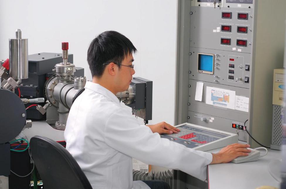
Magnetic-sector SIMS [ Cameca ims-6f ]
-
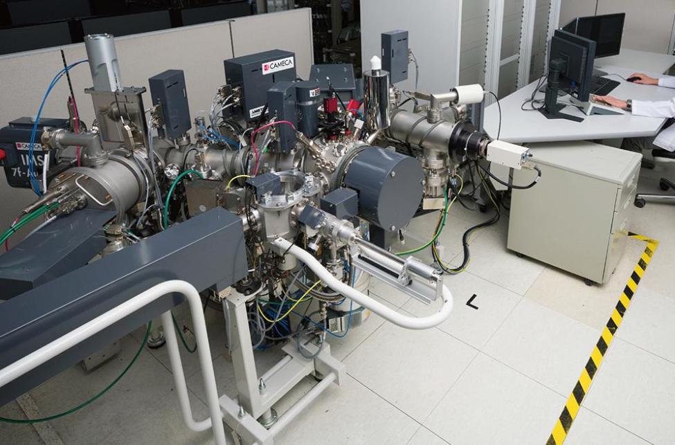
Magnetic-sector SIMS [ Cameca IMS 7f-Auto ]
-
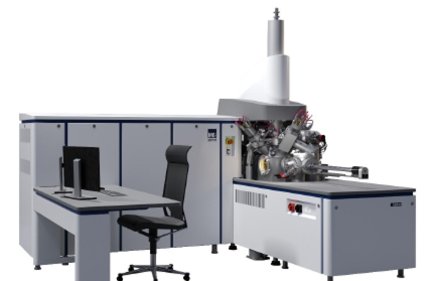
Time-of-Flight SIMS [ TOF-SIMS M6 plus, IONTOF GmbH ]
-
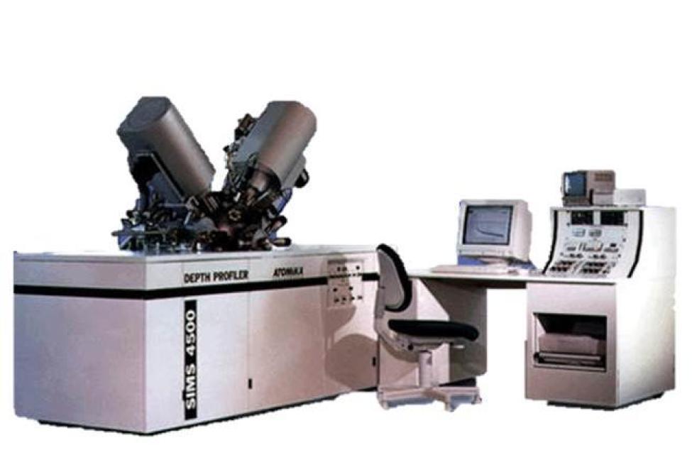
Quadrupole-SIMS [ CAMECA sims 4500 ]
Through a professional analysis team and advanced equipment, provide customers withHigh-precision and reliable material and process analysis services。
- High sensitivity elemental analysis capability
- nano-level depth resolution
- Advanced semiconductor doping analysis
- Organic and inorganic materials analysis
- IC process contamination and diffusion research
-
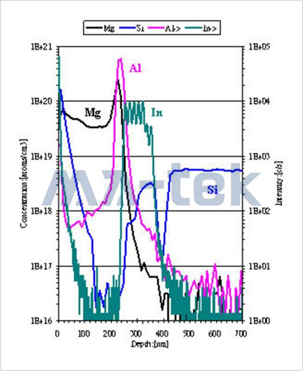
LED Analysis
-
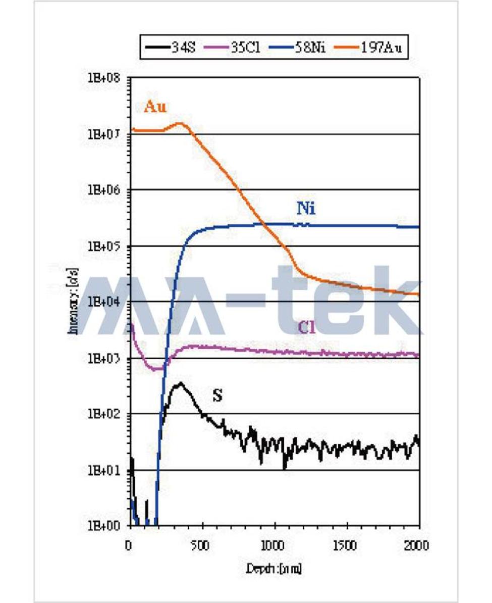
Analysis of Metal Pad Microcontamination in Spherical Array Packaging
-
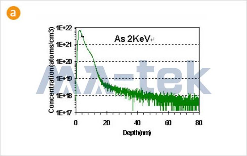
(a) Ultra-shallow junction ion implantation analysis
-
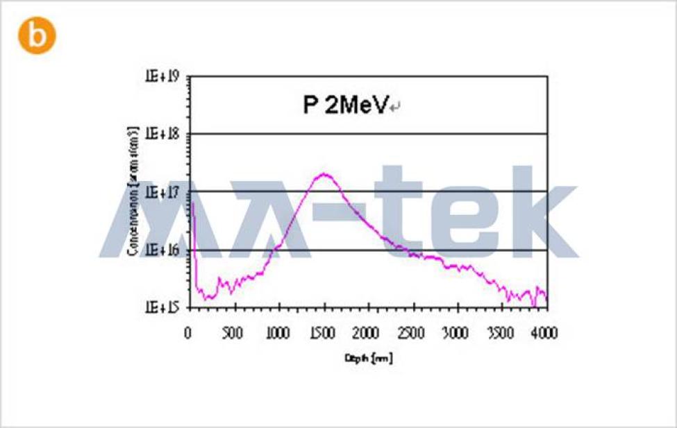
(b) Ultra-high energy ion implantation analysis
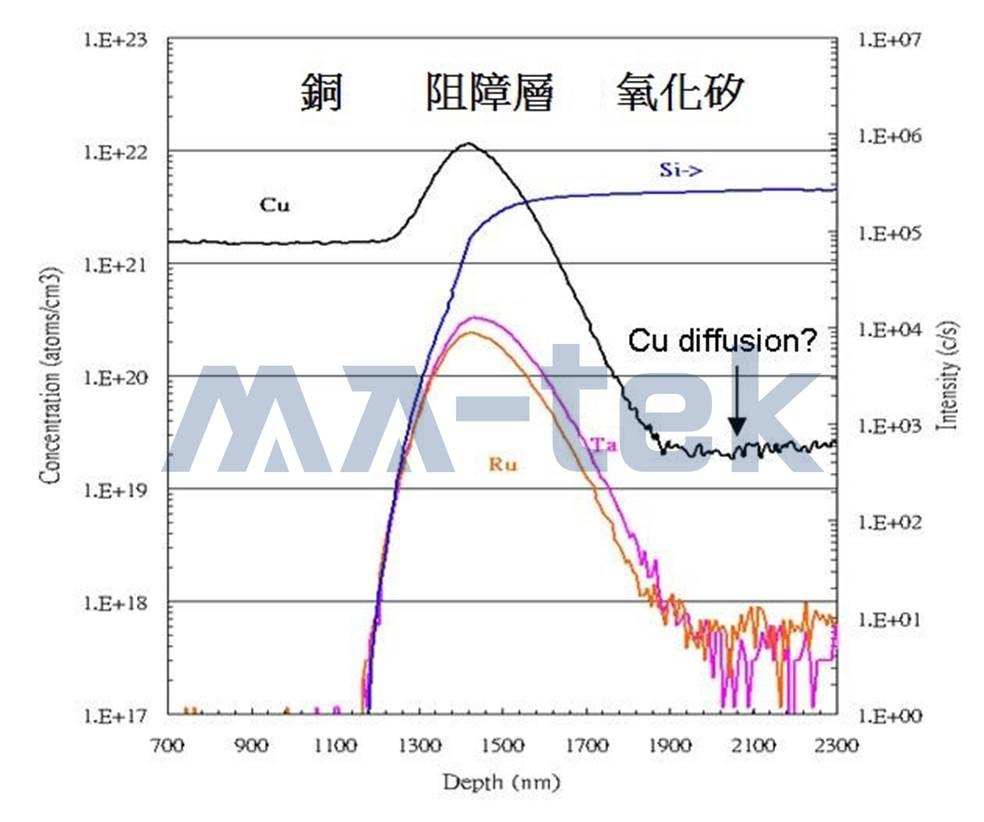
Front SIMS results:
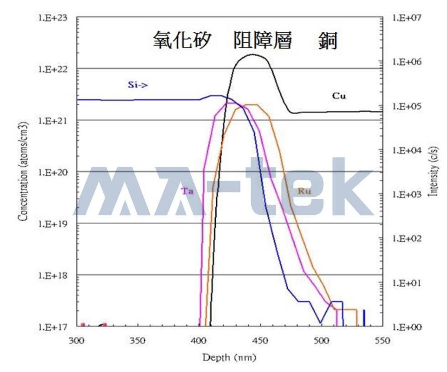
Back SIMS results:
-
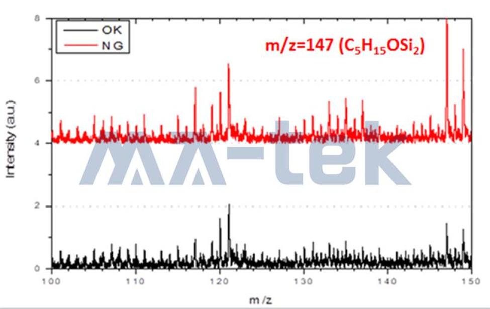
Silicon Oil contamination
-
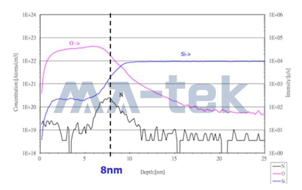
SiON film analysis
-
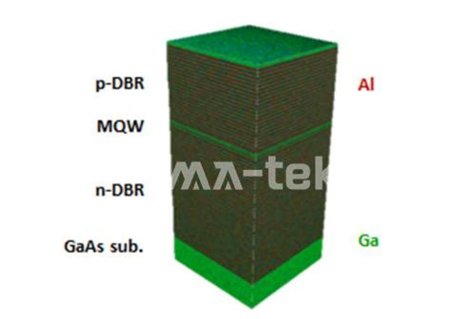
VCSEL 3D component distribution
-
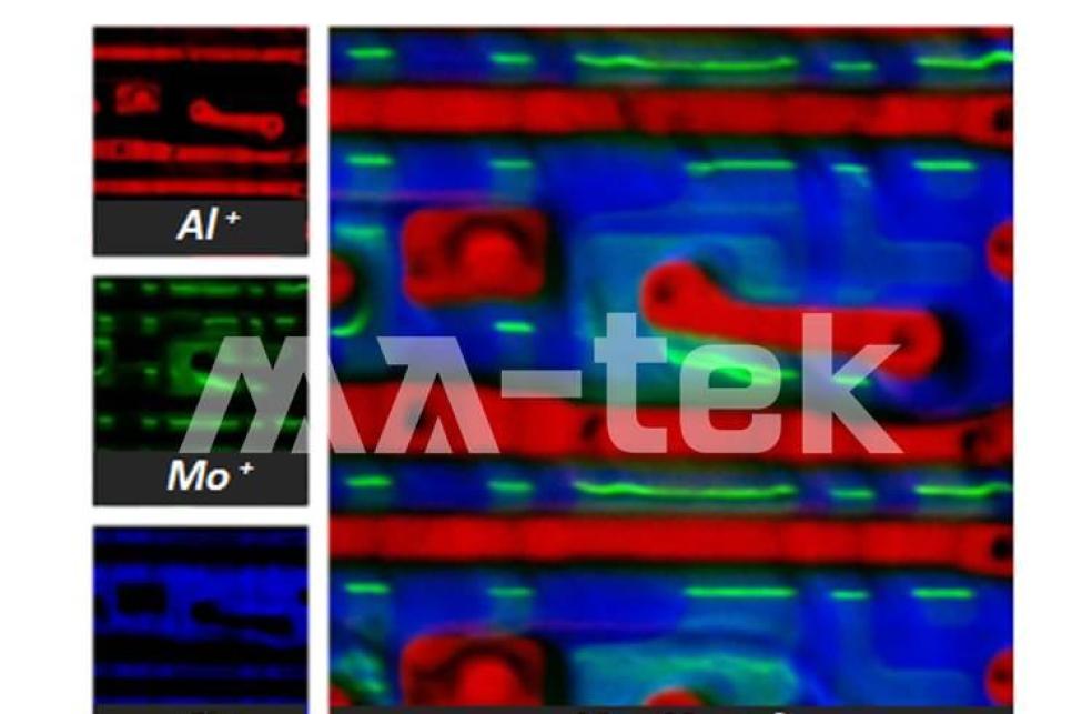
TFT planar component distribution


