

All Services
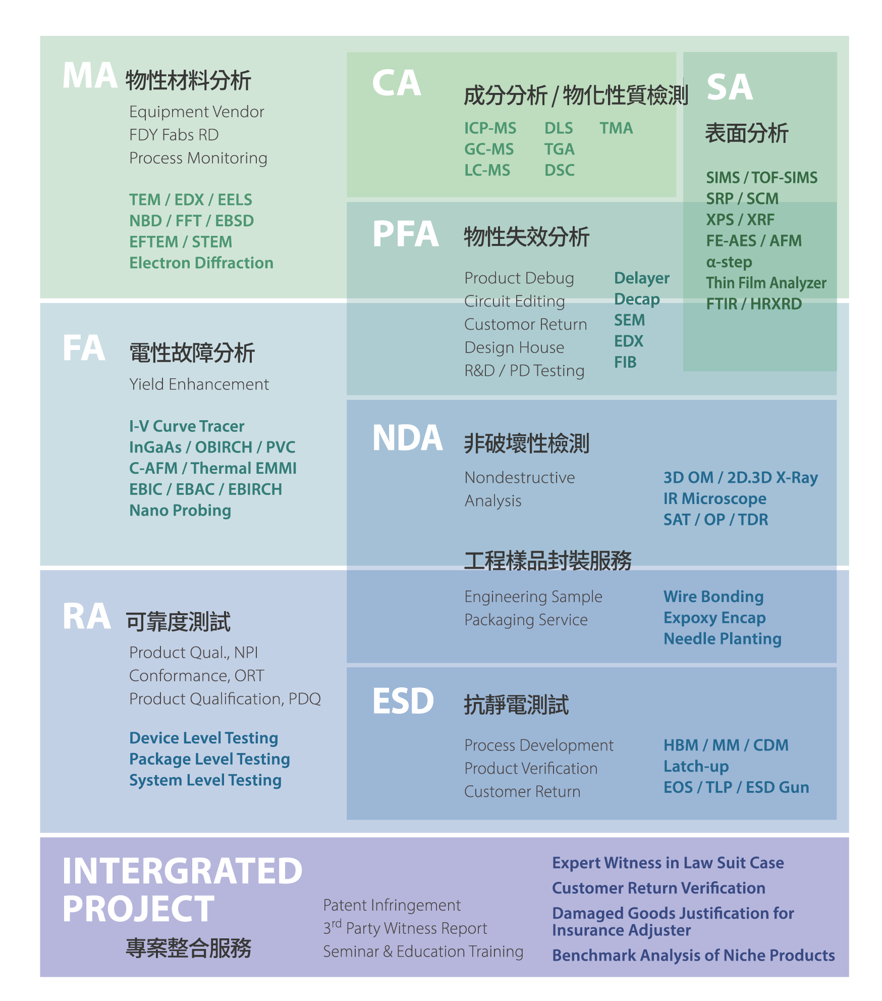
MA-tekMA-tek is Asia's leading semiconductor testing laboratory, focusing on Material Analysis (MA), Failure Analysis (FA), Surface Analysis (SA), Chemical Analysis (CA), and Reliability Testing (RA),Equipped with the most comprehensive instruments in the industry, including advanced machines such as TEM/EDX, SEM/EDX, and SIMS, and in line with AI and 2nm process development, high-power testing instruments (such as Incal/Sonoma, MCC/HPB6) are deployed.
- Comprehensive testing services: Provide failure analysis, material analysis, and reliability verification services to assist customers in improving product yield.
- Key technology leadership: Equipped with 2nmand below (sub-angstrom level) process testing capabilities have advantages in the fields of GAAFET, CPO silicon photonics, and 3D-IC technology.
- Global layout: Service locations span Taiwan (Hsinchu, Tainan), China (Shanghai, Xiamen, Shenzhen, Suzhou), and Japan (Nagoya, Kumamoto, Hokkaido).
- High efficiency service: Provides 24-hour data delivery, becoming an important partner in the global semiconductor supply chain.
-
SMT Surface Mount Technology Adhesive Services
Surface mounting technology is a fundamental process in the electronics industry, aimed at integrating various components with printed circuit boards (PCBs) to form a functional system. -
Board-level temperature cycling test
Board-level temperature cycling test is an important testing method used to assess the reliability of solder joints of surface-mounted components on printed circuit boards.
-
Board-level drop test
Board-level drop tests are primarily used to evaluate the reliability performance of assembled circuit boards when subjected to instantaneous mechanical shocks, with a particular focus on the structural integrity of the solder joints between surface-mounted components and the circuit board. -
Board-level unidirectional bending test
The board-level unidirectional bending test is a reliability testing method used to assess the structural integrity of electronic component solder joints under mechanical bending stress.
-
Board-level cyclic bending test
Board-level cyclic bending test is a mechanical durability testing method used to assess the fatigue life and reliability of solder joints of surface-mounted components under repeated bending stress, and is one of the important items in board-level reliability verification. -
Strain measurement
Strain measurement is a key technology that converts mechanical deformation into quantifiable engineering data, used to objectively quantify the degree of mechanical deformation that a circuit board undergoes during assembly, testing, and actual operation.
-
IC lifetime testing and early failure rate assessment
Lifetime testing is a crucial part of semiconductor component testing, used to assess the durability and failure modes of components under prolonged power-on conditions and high-temperature environments. -
Environmental stress testing
Environmental stress testing is a systematic verification of the reliability and durability of electronic components and products under extreme usage conditions, with the core purpose of confirming whether the assembly quality of the components is sufficient to support actual application requirements.
-
Mechanical Stress Test
Mechanical stress testing is used to assess whether the packaging structure, solder joints, and internal bonds of electronic components have sufficient mechanical strength and durability under external forces. -
PCB reliability testing
PCB reliability testing is a key verification to ensure that the circuit board can operate stably under harsh environments and long-term use conditions during manufacturing, assembly, reflow soldering, environmental stress, and prolonged use.
-
LED product lifespan testing
ED product lifetime testing is an important verification procedure for assessing the changes in optical characteristics and reliability of light-emitting diodes during long-term operation. -
ESS Environmental Stress Screening
Environmental stress screening is aimed at exposing potential defects in advance, revealing latent defects that cannot be detected through functional testing in the normal production process, eliminating early defective products, and ensuring that the final shipped products achieve higher reliability and stability.
-
MST mechanical stress test
Sources of mechanical stress include dropping, vibration, compression, pulling, impact, and bending. -
EST environmental stress test
Environmental stress testing evaluates whether a product can maintain stable operation under various extreme conditions simulated from real usage environments, such as high temperatures, low temperatures, humidity changes, temperature cycling, corrosion, dust, and sunlight exposure.
-
ESD electrostatic protection testing and design services
Electrostatic discharge is to avoid interface damage, chip burning, or product failure caused by external static electricity. Complete electrostatic protection testing, electrostatic protection design, and latch-up verification must be conducted during the design phase and mass production phase. -
Automotive Component Reliability Services
Automotive component reliability services are a series of verification and testing services conducted on the "reliability" and "durability" of automotive electronic components used in actual application environments over a long period.
-
PEM-CCD
PEM-CCD, also known as EMMI, is a widely used non-destructive hotspot localization technology. Its principle is to detect the weak photons released due to electron-hole recombination or thermal carrier effects when the IC is in operation. -
InGaAs Gallium Arsenide Indium Micro-Optical Microscope
The detection principle of PEM-InGaAs is to detect the photons emitted from the recombination of electrons and holes, as well as from thermally excited carriers. By detecting the weak photons released due to leakage current, abnormal conduction, or thermal carrier effects in the powered state through the detection IC, the failure location inside the chip can be quickly pinpointed.
-
C-AFM Conductive Atomic Force Microscope
C-AFM (Conductive Atomic Force Microscopy) is a high-resolution electrical analysis technique based on atomic force microscopy, which combines a conductive probe with a bias application mechanism to achieve simultaneous measurement of surface morphology and local current signals. -
AFM nano-probe electrical measurement technology
AFM nano-probe electrical measurement technology is based on atomic force microscopy (AFM) with high spatial resolution, combined with a multi-probe nano-electrical detection system, to directly perform electrical measurements and failure localization on a single transistor at the nanoscale, a non-destructive analysis technique.
-
SEM-based Nano-probing
SEM-based Nano-probing can be performed in a SEM vacuum environment using a low acceleration voltage (Low kV) electron beam combined with a nano probe, and has been successfully applied in the 5nm FinFET process node.
-
Thermal EMMI
Thermal EMMI is a high-sensitivity failure analysis technique that locates defects by detecting the minute thermal radiation generated by components under powered conditions.
-
OBIRCH laser beam resistance anomaly detection
IR-OBIRCH is a non-destructive failure analysis technique that scans the surface (or back) of ICs using infrared laser, inducing localized heating to cause resistance changes, thereby detecting abnormal conduction or leakage locations. -
EBIRCH electron beam induced resistance change technology
EBIRCH electron beam induced resistance change technologyAble to detect areas of abnormal resistance in the circuit and accurately locate defect positions in the internal metal interconnects, Poly, or Contact layers of the IC.
-
EBAC electron beam-induced current analysis technology
EBAC electron beam-induced current technology is one of the important electrical localization tools in scanning electron microscopy (SEM) failure analysis, particularly suitable for analyzing conduction issues in metal interconnect structures. -
EBIC electron beam-induced current analysis technology
EBIC (Electron Beam Induced Current) analysis technology is one of the important electrical localization methods in SEM failure analysis.
-
SAT ultrasonic scanning microscope
SAT ultrasonic scanning microscopy is commonly used to detect various hidden defects inside the package, such as delamination, voids, cracks, chipping, uneven resin, and bonding anomalies.
-
3D OM Optical Microscope
3D OM optical microscope utilizes principles such as optical interference, focal plane stacking, or white light interference to obtain three-dimensional height information (Z-axis) of samples in a non-destructive manner, while simultaneously presenting high-resolution 2D × 3D structural images.
-
fluorescence microscope
Fluorescence microscopy analysis mainly utilizes fluorescence penetration experiments (Fluorescent Penetrant Inspection, FPIConduct defect observation. -
OM Optical Microscope
Optical microscopy uses visible light to illuminate the surface of samples, quickly revealing the macroscopic morphology of components, materials, and structures through reflection, scattering, and optical contrast differences, providing important reference points for subsequent analysis.
-
OP White Light Interferometer
White light interferometer mainly utilizes the principle of white light interferometry for surface measurement. -
TDR Time Domain Reflectometer
Time Domain Reflectometry (TDR) is an analysis technique that uses the reflection characteristics of electrical signals for impedance measurement and fault location.
-
3D X-ray
3D X-ray (High Resolution 3D X-ray Microscope) obtains multi-angle images by rotating the sample and uses computer reconstruction to create a three-dimensional structure, allowing engineers to observe internal defects from different angles and even perform virtual slice analysis. -
2D X-ray
2D X-ray is a technique that uses X-rays generated by high-energy impacts on a metal target, which have penetrating properties, to observe and determine whether there are issues such as cold solder joints, HIP, or Hop inside advanced packaging without damaging the sample.
-
SEM scanning electron microscopy
Scanning electron microscopy, also known as scanning electron microscope, is a high-resolution microscopic analysis technique that uses a high-energy electron beam to scan the surface of a sample and forms images based on signals generated from the interaction between electrons and the material. -
TEM transmission electron microscope
Transmission Electron Microscope (TEM), also known as transmission electron microscope, is a high-resolution microscopic analysis technique that uses a high-energy electron beam to penetrate ultra-thin samples and form images.
-
FIB focused ion beam microscope
Focused Ion Beam (FIB) is a precision analysis technique that uses high-energy ion beams for nanoscale processing, cross-section preparation, and microstructure analysis of materials. -
DB P-FIB Dual Beam Focused Ion Beam
Dual Beam Plasma FIB (DP-FIB) is a high-performance material processing and analysis equipment that combines plasma ion beam and scanning electron microscopy (SEM).
-
EBSD Electron Backscatter Diffraction
Electron Backscatter Diffraction (EBSD) is an important microscopic analysis technique that uses electron diffraction signals to analyze the crystal structure and grain orientation of materials. -
EELS electron energy loss spectrum
Electron Energy Loss Spectroscopy,EELSis a high-resolution material analysis technique that combines transmission electron microscopy (TEM) or scanning transmission electron microscopy (STEM).
-
SIMS Secondary Ion Mass Spectrometer
Secondary Ion Mass Spectrometry (SIMS) is a highly sensitive material analysis technique widely used in semiconductor process analysis, materials research, elemental distribution measurement, and trace contamination analysis. -
XPS X-ray Photoelectron Spectrometer
X-ray Photoelectron Spectroscopy (XPS) is a highly sensitive surface analysis technique used to measure the elemental composition and chemical bonding states of material surfaces.
-
XRF X-ray fluorescence spectrometer
X-ray fluorescence analysis (XRF) is a non-destructive elemental analysis technique. -
AES OJE Electronics Energy Spectrum Analyzer
Auger Electron Spectroscopy (AES) is a high-resolution surface elemental analysis technique that can be used to analyze the elemental composition and chemical states of extremely thin layers on material surfaces.
-
FTIR Fourier Transform Infrared Spectroscopy
Fourier Transform Infrared Spectroscopy (FTIR) is a spectroscopic technique that utilizes the infrared light absorption characteristics for the analysis of organic components in materials. -
HRXRD High-Resolution X-ray Diffraction Analyzer
High-Resolution X-ray Diffraction (HRXRD) utilizes the Bragg Diffraction phenomenon produced when X-rays irradiate crystalline materials. By analyzing the diffraction angles and intensity distribution, the crystal structure and crystallization characteristics of the material can be obtained.
-
AFM atomic force microscope
Atomic Force Microscope (AFM) is a high-resolution scanning probe microscopy technique that can be used to measure the nanoscale morphology and structural features of material surfaces.
-
α-step thin film thickness profiler
The film thickness profile measurement instrument (α-Step) is a precision device that uses a mechanical probe to scan and measure surface profiles. The system employs a diamond-tipped stylus to perform linear scanning on the sample surface.
-
Optical Film Thickness Measurement Instrument
It is a non-contact analysis technique for measuring film thickness using Optical Reflectance Spectroscopy. -
SRP impedance analysis instrument
The Surface Resistance Probe (SRP) is a commonly used electrical measurement technique in semiconductor material analysis, capable of measuring the depth distribution of junction depth, resistivity, and effective carrier concentration. It is widely applied in ion implantation and process monitoring analysis.
-
SCM scanning capacitance microscopy
Scanning capacitance microscopy (SCM) is a semiconductor analysis technique based on scanning probe microscopy (SPM) that can be used to observe the two-dimensional doping distribution in materials and can clearly distinguish between N-type and P-type regions.
-
Chemical mass spectrometry analysis
Mass spectrometry (MS) is a highly sensitive analytical technique widely used in materials analysis, semiconductor analysis, environmental monitoring, biomedical research, food testing, and chemical research.
-
Inductively Coupled Plasma Mass Spectrometer
Inductively Coupled Plasma Mass Spectrometry (ICP-MS) is a highly sensitive elemental analysis technique primarily used for determining trace elements and isotopic composition in samples. -
LC-MS / MS liquid chromatography / mass spectrometer
LC-MS/MS is an analytical technique that combines liquid chromatography (LC) and mass spectrometry (MS) in tandem, integrating the high separation efficiency of liquid chromatography with the high sensitivity mass analysis capability of mass spectrometry.
-
Dry etching and grinding for layer removal
Dry etching and delayering are methods that remove the metal layers and dielectric layers inside integrated circuits (IC) layer by layer through ion dry etching, chemical etching, or mechanical grinding. -
Laser etching to remove encapsulant
Laser decapsulation is a non-contact process commonly used in failure analysis (FA) sample preparation techniques.
-
Chemical etching to remove encapsulant
Chemical Decapsulation is a commonly used sample preparation technique in Failure Analysis (FA) of semiconductor devices. -
TEM sample preparation
Transmission Electron Microscope,TEMis a high-resolution analytical technique capable of observing structures at the nanoscale or even atomic scale.
-
Laser Ball Placement
Laser re-balling technology is a non-contact laser heating and single ball control method that can precisely complete solder ball bonding in a small area, significantly reducing thermal impact and mechanical stress, making it an important solution for advanced packaging and analysis applications. -
Repair workstation
In the process of semiconductor packaging and electronic product development, when a component malfunctions and needs to be replaced or further analyzed, Rework technology becomes an indispensable key process.
-
IC packaging wire bonding service
Wire Bonding is an important technology for establishing electrical connections between the die and external circuits or package pins. -
CP Ion Polishing
Ion Milling, also known as Cross-Section Polishing (CP), is a sample preparation technique that uses a high-energy ion beam to bombard the surface of a sample, removing material and forming a smooth cross-section.
-
FIB circuit repair
FIB uses gallium (Ga, atomic number 31) as an ion source, utilizing a negative electric field applied to the extractor to pull gallium atoms from the tip, forming a gallium ion beam. The beam is focused through an electric lens, and the size of the ion beam can be determined by a series of variable apertures, ultimately focusing the ion beam onto the surface of the sample. -
Integrated Project Services
MA-tek, with its solid analytical technology foundation and rich practical experience, provides a range of services including patent evaluation, third-party reporting, laboratory setup, technology transfer, and training, assisting clients from "problem analysis" to "capability building" to create long-term competitive advantages.
-
Failure Analysis Solution Process
MA-tek combines years of materials analysis and failure analysis experience to establish a complete and standardized failure analysis process, from preliminary information collection, non-destructive testing, to electrical localization and physical analysis, providing a one-stop and highly efficient analytical solution to assist customers in quickly clarifying issues and shortening product development and verification timelines. -
Competitive Product Analysis
MA-tek assists customers in deeply analyzing the internal structure, circuit layout, and key processes of products through systematic IC imaging and reverse engineering techniques, providing concrete and feasible technical insights.


