
OP White Light Interferometer
The white light interferometer (Optical Profilometer, OP) is based onoptical interference principleHigh-resolution measurement technology for surface morphology measurement, through the analysis of white light interference signals, can reconstruct the three-dimensional structure of material surfaces and measure height differences and surface roughness on a micron to nanometer scale.It is a non-contact, non-destructive measurement methodcan quickly obtain high-precision three-dimensional surface information without damaging the sample, and is therefore widely used in the fields of semiconductors, optoelectronics, precision machinery, and materials science.Through the white light interferometer, measurements can be conducted.Surface roughness measurement,step height measurement,Waviness analysis,Three-dimensional surface morphology analysis,Measurement of microstructure height and dimensions.
MA-tekLong-term dedication to the fields of material analysis and semiconductor failure analysis has established a complete surface morphology measurement and material analysis platform, providing high-precision three-dimensional surface measurements and professional data interpretation. Through multi-technology integration, a complete analysis process is conducted.
-
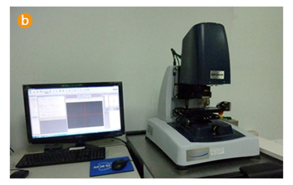 Image | Bruker Contour GT White Light Interferometer
-
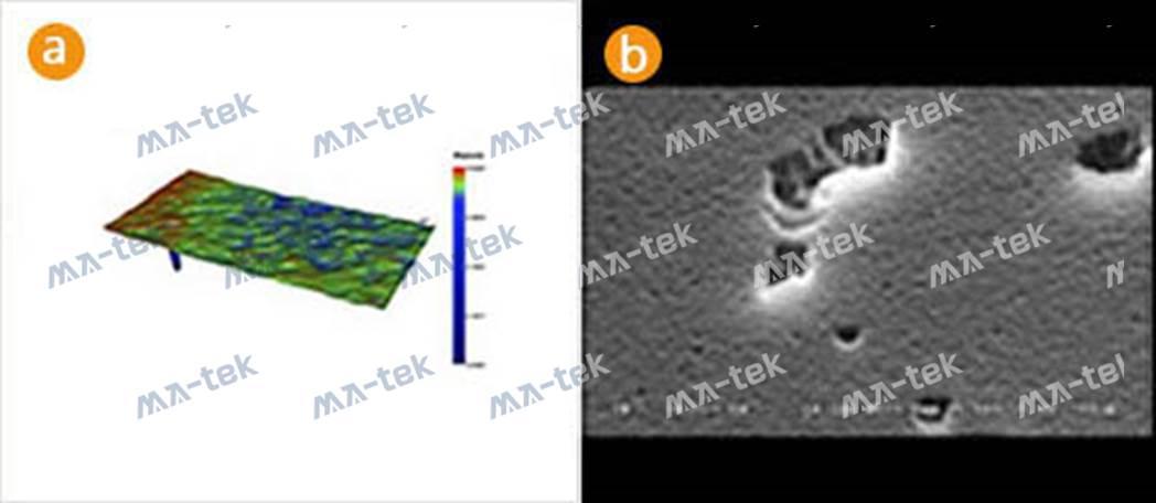
Figure | Surface Defect Morphology Analysis: The white light interferometer can identify depressions, holes, and microstructural defects on the material surface.
(a) Optical Interference Profilometer 3D Surface Image
(b) SEM secondary electron microscope corresponding image -
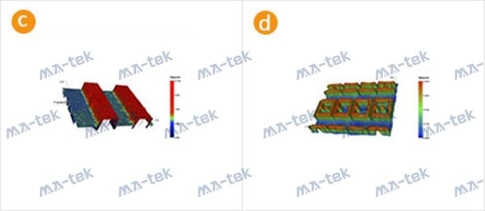
Figure | Microstructure size and height measurement: The white light interferometer can accurately measure the height and morphology of metal structures.
(c) Flexible Printed Circuit Board (FPC) Gold Finger Structure
(d) Measurement of photomask chromium metal film patterns
-
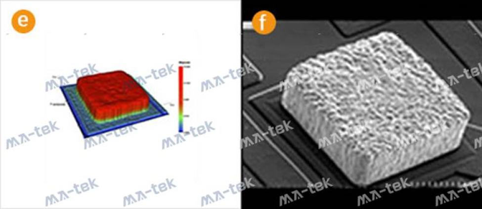
Figure | Gold bump morphology analysis: bump height, bump uniformity, bump surface roughness.
(e) White light interferometer three-dimensional measurement image
(f) SEM secondary electron microscope image -
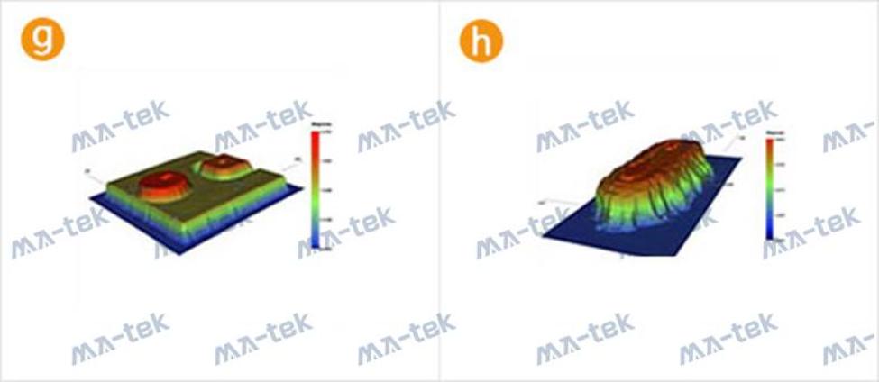
Figure | Surface structure measurement of optoelectronic components
(g) LED chip metal electrode morphology
(h) TFT panel Photo Spacer height measurement
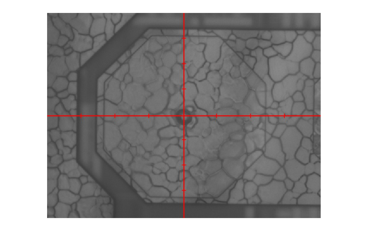
The white light interferometer mainly utilizes the principle of white light interferometry for surface measurement. When white light is illuminated on the sample surface, part of the light is reflected by the sample surface, while another part is reflected by the reference mirror. The two beams of light superimpose again to form interference fringes. By scanning the sample height and analyzing the changes in the interference signal, the system can calculate the height information at each position, thereby reconstructing a complete three-dimensional surface morphology. The measurement modes include:
- Vertical Scanning Interferometry (VSI): Suitable for samples with larger surface undulations, capable of measuring height differences from micrometers to tens of micrometers, commonly used for packaging structures or microelectromechanical component analysis.
- Phase Shifting Interferometry (PSI): Suitable for samples with relatively flat surfaces, it can provide nanometer-level height resolution and is commonly used for surface roughness and thin film measurements.
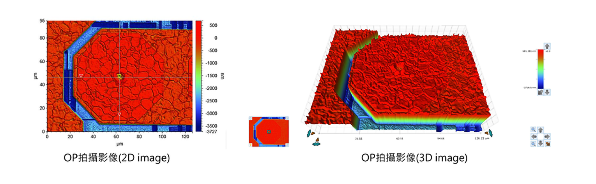
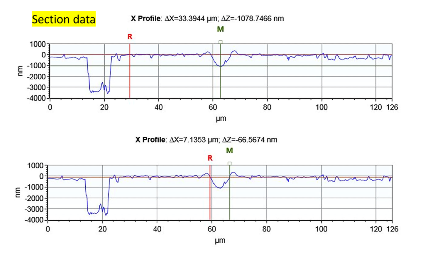
The white light interferometer can provide three-dimensional surface morphology, surface roughness, step height measurement, and waviness analysis.
The white light interferometer has a wide range of applications in the electronics and optoelectronics industries, particularly suitable for measuring the surface morphology of microstructures.
-
Semiconductor and Packaging
-
Gold bump height measurement
-
Wafer surface roughness
-
Microstructure step height measurement
-
-
PCB and electronic components
-
FPC gold finger height measurement
-
PCB surface structure inspection
-
-
optoelectronic industry
-
LED surface roughness
-
TFT panel Photo spacer measurement
-
-
Materials and Films
-
Film thickness difference
-
Surface defect analysis
-


