
EBAC electron beam absorption current analysis technology
As the semiconductor process nodes continue to shrink, the internal metal interconnect structure of chips has become more complex. Modern logic chips typically include multi-layer metal interconnect architectures, such as Metal 1 to Metal 10 or even higher levels, responsible for connecting transistors and circuit modules. However, in advanced processes, process scaling and high-density layouts have also increased the risk of metal line failures, such as metal opens, high resistance, or poor contacts.
EBAC (Electron Beam Absorbed Current) technologyIt is one of the important electrical localization tools in scanning electron microscope (SEM) failure analysis, particularly suitable for analyzing conduction issues in metal interconnect structures. Through electron beam scanning and current measurement, EBAC can quickly identify the location of conduction interruptions in the circuit, enabling engineers to effectively locate open circuit or high impedance defects and further conduct subsequent physical analysis.
EBAC analysis is performed in a SEM environment. When the electron beam scans the chip surface, it can penetrate the protective layer and the interlayer dielectric (ILD), generating electron signals in the metal wires. If the metal wires are in a normal conductive state, the charges generated by the electron beam can be extracted and measured through the current loop formed by the probe.
However, when there are open circuit defects or high-resistance areas in the metal wires, the current conduction will be interrupted at the defect location, causing a significant change in the EBAC current signal in that area. Through the spatial distribution images of the current signals, engineers can quickly determine the conduction status of the wires and locate the defect position. Due to the high-resolution scanning capability of the electron beam, even if the metal wires are located beneath other metal wires,EBACIt can effectively trace the conduction path and identify the location of circuit interruptions, thus it is widely used in advanced process failure analysis.
In the development and mass production process of semiconductor products, metal interconnect defects are one of the common sources of failure. The EBAC technology, through electron beam induced current measurement, can quickly locate open circuits or high impedance defects in metal wires at the nanoscale, thus playing an important role in the failure analysis process. EBAC is often used to analyze:
- Metal Open Defect:When metal wires break or process defects cause a disruption in conductivity, EBAC can accurately locate the open circuit position.
- High Resistance Contact:If the resistance of the metal contact point increases abnormally, the current signal variation will also be presented in the EBAC image, assisting engineers in determining the source of the problem.
- Multi-layer metal interconnection failure:EBAC can trace the conductive paths of multi-layer metal interconnections and identify the defect locations within the deep wires.
In advanced process IC failure analysis, a single analysis technique often struggles to completely locate defects. Different types of defects, such asOpen, Short, Leakage or High Resistanceneeds to be combined with different electrical localization techniques for cross-validation.
MA-tekThrough integrationEBIC, EBAC, EBIRCH and OBIRCHAdvanced positioning technologies can quickly identify defect locations for different failure modes and further confirm root causes by combining with physical analysis methods such as FIB and TEM.
As the process node advances5nm, 3nm, and even 2nmThe internal structure of the chip has become more complex, and defect locations are often found in deep metal layers or at the nanoscale junctions.
Through the cross-application of different analysis techniques, it is possible to:
-
Increase the success rate of defect localization
-
reduce misjudgment
-
shorten analysis time
-
Improve the success rate of subsequent FIB / TEM sample preparation.
Therefore, in advanced process failure analysis,EBIC, EBAC, EBIRCH and OBIRCHhas become an indispensable electrical localization tool.
| analysis technology | Main Principle | Applicable defect types | Application |
|---|---|---|---|
| EBIC | The electron beam generates electron-hole pairs and forms a current image. | Junction leakage、Gate oxide breakdown | Interface defect localization, oxide layer breakdown analysis |
| EBAC | Electron beam excites the current in the metal wire and tracks the conduction path. | Metal open, High resistance | Multi-layer metal interconnect open circuit localization |
| EBIRCH | The electron beam causes localized temperature rise, resulting in resistance changes. | Metal short, High impedance | Metal short circuit and high impedance defects |
| OBIRCH | Laser localized heating causes resistance change. | Short-circuit defects, leakage paths | Packaging and Chip Short Circuit Localization |
As the semiconductor process nodes continue to shrink, the reliability of multilayer metal interconnect structures increasingly impacts chip performance and yield. The EBAC (Electron Beam Absorbed Current) technology utilizes the current signals generated by the interaction between the electron beam and metal wires, allowing for rapid localization of open and high-impedance defects at the nanoscale, and has become a key tool in the failure analysis process of advanced manufacturing.
MA-tekLong-term deep cultivation in the field of semiconductor material analysis and failure analysis has established a complete advanced process analysis platform. In the application of EBAC technology, MA-tek can combine multiple electrical and material analysis techniques to provide more comprehensive defect localization and root cause analysis capabilities through integration:
-
SEM-based Nano-probing
-
EBIC / EBIRCH Electron Beam Induced Analysis
-
OBIRCH laser resistance variation localization
-
C-AFM conductive atomic force microscope
-
FIB precise cross-section sample preparation
-
TEM nano structure analysis
This can form, from Electrical defect localization → Structural analysis → Material root cause verificationThe complete failure analysis process. Through cross-technology integration and professional interpretation capabilities, it can effectively shorten positioning time and improve analysis success rates, providing efficient and highly credible analysis solutions for advanced processes and high-reliability products.
-
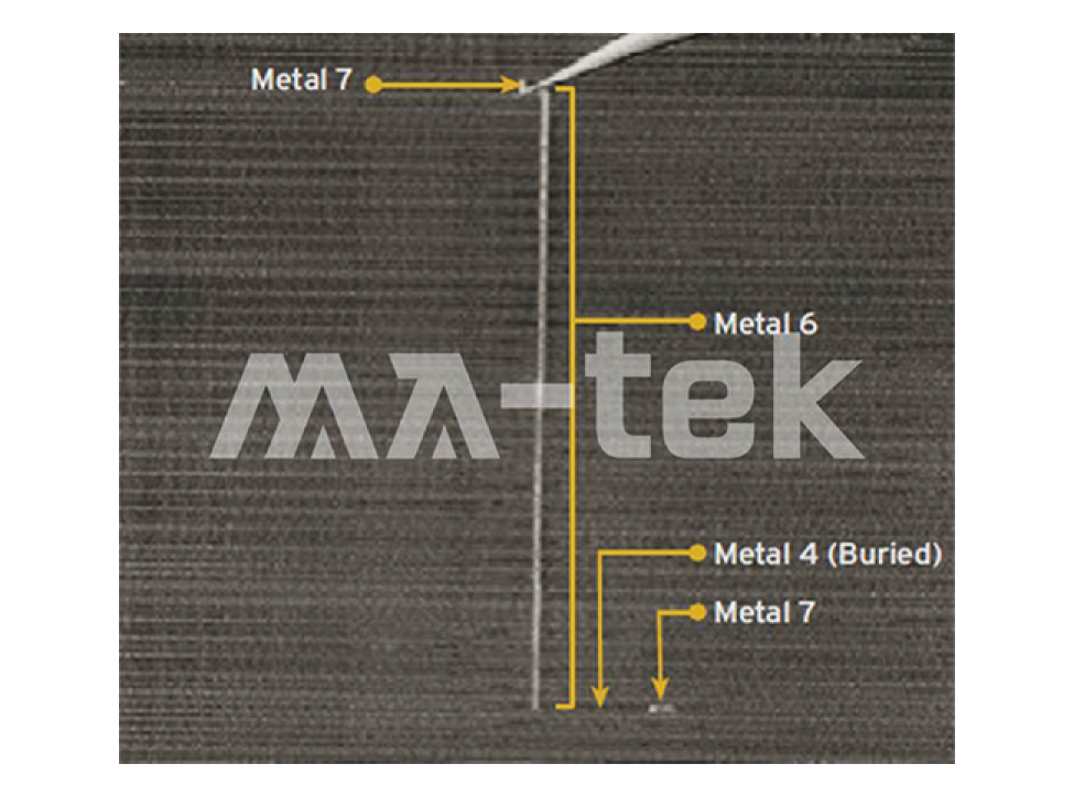 Figure | EBAC can locate open defects in multi-layer metal interconnects.EBAC (Electron Beam Absorbed Current) technology can be used to analyze the conduction paths and defect locations in multilayer metal interconnect structures. In a SEM environment, when the electron beam scans the metal wires, it generates an absorbed current within the wires, which is measured through the current loop formed by the probe. When there is an open circuit or high impedance defect in the metal wire, the current conduction will be interrupted at the defect location, resulting in a significant contrast in that area in the EBAC image. This technology can effectively identify.Metal 7, Metal 6, and even metal layers buried in the dielectric layerhas important value in advanced process interconnect failure analysis.
 -
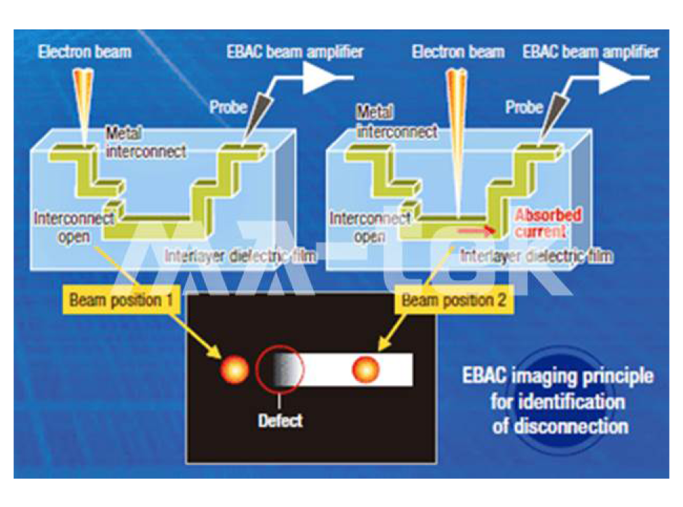 Diagram | EBAC (Electron Beam Absorbed Current) technology principle schematicEBAC technology uses the absorbed current signal generated when scanning metal wires with a SEM electron beam to locate defects. When the electron beam irradiates a conductive metal line, the charges generated by the electron beam can be extracted through the current loop formed by the probe; if there are open circuit or poor contact defects in the line, the current will be interrupted at the defect. By measuring the changes in the electron beam induced current, the metal interconnects can be located in the EBAC image.open defect or high impedance areaand quickly locate the circuit failure position.


