
Competitive Product Analysis
In the rapidly evolving market of semiconductors and electronic products, understanding the design architecture and process technology of competing products has become an important foundation for companies to formulate strategies and accelerate research and development. MA-tek utilizes systematicIC imaging and reverse engineering technologyto assist customers in deeply analyzing the internal structure, circuit layout, and key processes of products, providing specific and feasible technical insights, which are not only applicable to technology development and product optimization but also widely used in market research, cost analysis, and patent strategy formulation, making it an indispensable analytical tool for enterprises in a highly competitive environment.
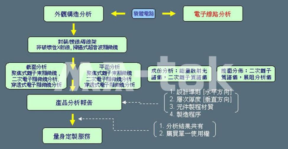
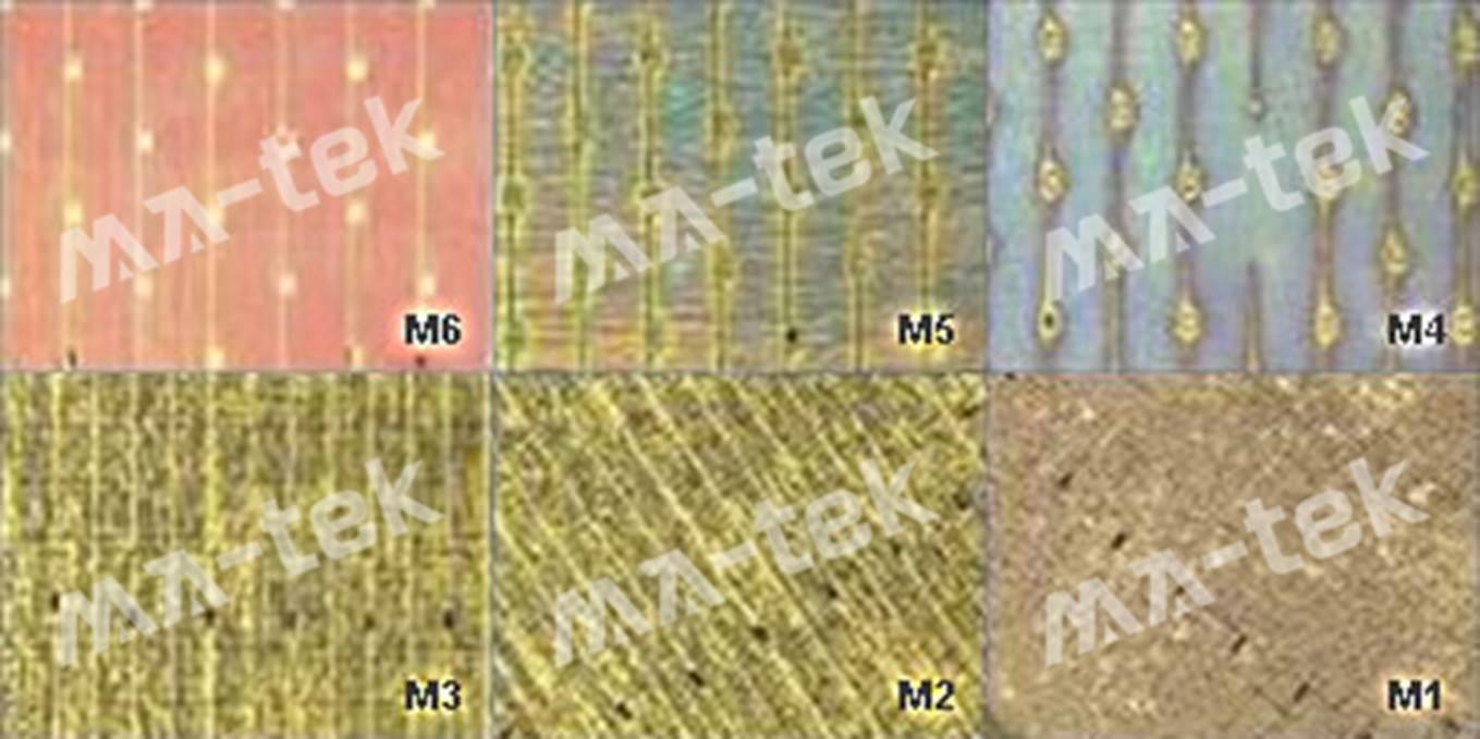
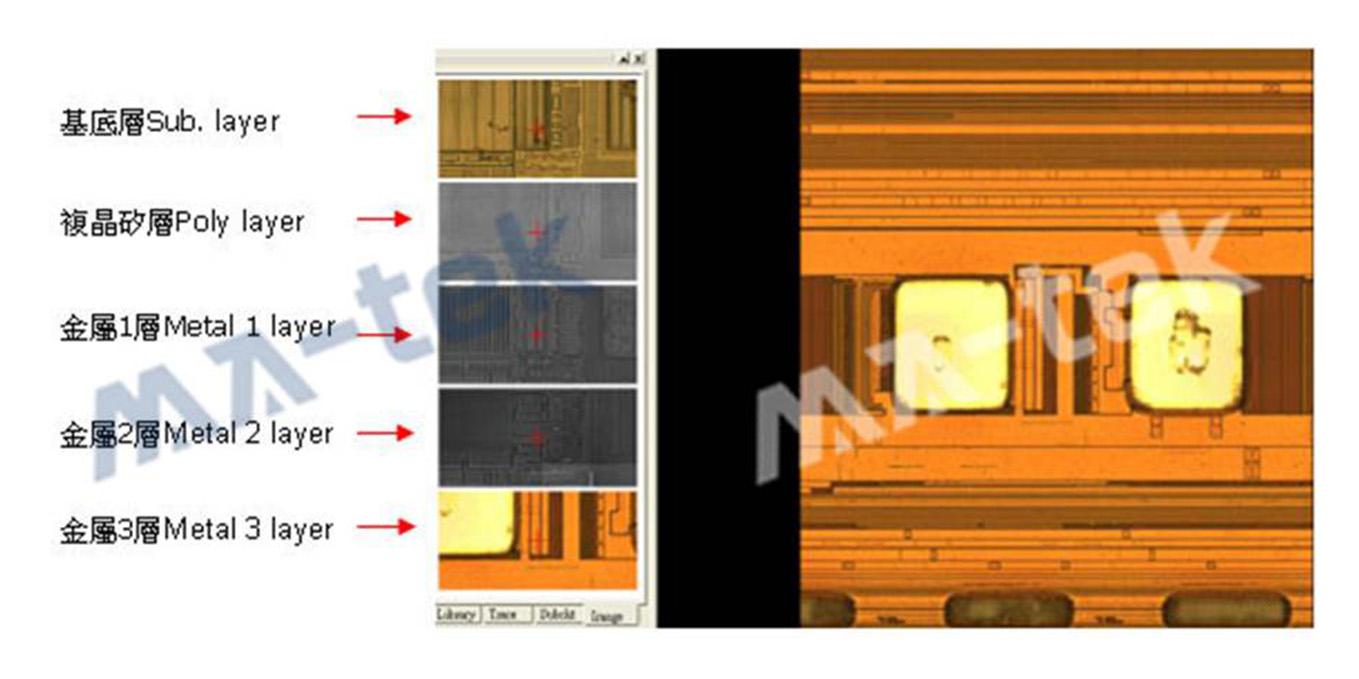
Through the delayering technology, the IC structure is restored layer by layer, combined with optical microscopy (OM) and scanning electron microscopy (SEM) for high-resolution image capture, and through automatic stitching and image alignment technology, a complete circuit layout and interlayer relationships are established.Through systematic restoration, not only can we "see" the structure, but we can also "understand" the design thinking and process strategies.
-
Multi-layer metal structures (M1 to M6) and wire configurations
-
Poly / Active / Via and other key structures
-
Layer thickness, material distribution, and process characteristics
-
Circuit connection relationships and design logic

-
Through precise delayering processes, metal and dielectric layer structures are removed layer by layer, avoiding excessive etching or damage to critical features.
- Then, through high-resolution microscopic imaging (OM / SEM) for continuous shooting and stitching, a complete image database is established.
- Finally, through circuit reconstruction and analysis technology, the images are converted into analyzable circuit structures, assisting customers in circuit extraction, significantly shortening design analysis time and improving analysis accuracy.
The value of competitive product analysis lies not only in technical analysis but also in supporting corporate decision-making. Through complete IC photography and structural analysis, MA-tek can assist clients in directly transforming analysis results into R&D strategies and market competitive advantages.
-
Evaluate the development direction and feasibility of new product technology.
-
Perform design debugging and problem localization
-
Establish cost structure and process evaluation model
-
Analyze the design differences and technical advantages of competing products.
-
Support patent clause analysis and infringement risk assessment
Through the delayering technology, MA-tek can fully analyze multilayer metal structures and polycrystalline silicon layers, and conduct detailed observations on the copper damascene process. Such analysis can reveal process design rules, interlayer relationships, and material selection strategies, providing a basis for process optimization and technology comparison.
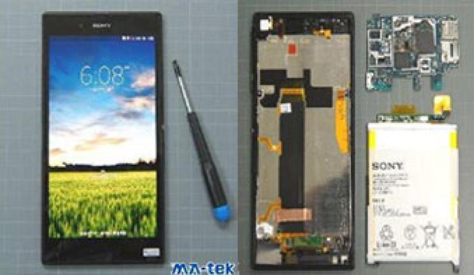
Taking the Sony Xperia Z Ultra as an example, through systematic disassembly and analysis, one can fully grasp its core architecture and key technologies. Through such Benchmark analysis, customers can quickly understand the mainstream technology direction in the market, serving as an important reference for product development and technology layout.
-
Using Qualcomm Snapdragon 800 quad-core processor
-
with ELPIDA 2GB LPDDR3 memory (PoP packaging)
-
The process uses 28nm HKMG technology.
-
Emphasize high performance and low power consumption design
-
-
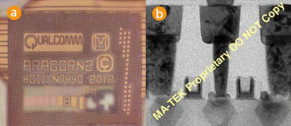
(a) Die Mark: Used for identifying chip source and process information
(b) PMOS structure: presents the design features of the transistor channel and gate.


