
SRP impedance analyzer
Technical Principles
Spreading Resistance Profiling (SRP) is a commonly used electrical measurement technique in semiconductor material analysis, which can measure the depth distribution of junction depth, resistivity, and effective carrier concentration. It is widely applied in ion implantation and process monitoring analysis.
The measurement principle of SRP utilizes two microprobes that contact the sample surface and apply a small voltage, measuring the resistance value between the probes, and converting it through calculations to obtain the resistivity and carrier concentration distribution of the material. Before analysis, the sample is fixed on a base with a slight tilt angle and is precisely polished using diamond grinding paste to gradually expose the semiconductor junction, forming a sloped cut surface. As the probes measure point by point along the polished surface, the resistivity and carrier concentration distribution in the depth direction of the material can be obtained, allowing for the analysis of the junction characteristics of semiconductor devices. SRP is often used in conjunction with material analysis techniques such as SIMS to simultaneously obtain information on element concentration and electrical distribution.
Analysis Application
Process Monitoring and Analysis
Electrical characteristic monitoring and process optimization applicable to ion implantation and annealing processes.
Deep junction concentration distribution analysis
Quickly obtain the carrier concentration distribution in the deep junction structure.
Contact Surface Depth Analysis
Accurate measurement of the P-N junction depth of semiconductor devices.
Effective carrier concentration depth profiling
Measuring the distribution of effective carrier concentration in semiconductor materials with depth.
Types of machines
-
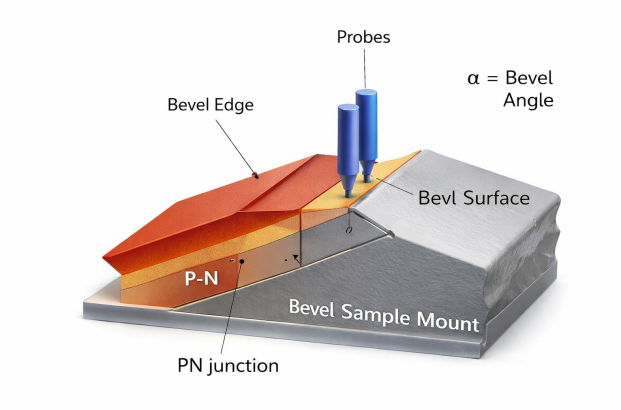
SRP measurement principle diagram
The semiconductor wafer is precision ground to form a bevel surface, allowing the P-N junction to be exposed along the surface direction. Two micro-probes contact the ground surface and apply a small voltage to measure the resistance between the probes, from which the resistivity and carrier concentration distribution of the material can be calculated. -
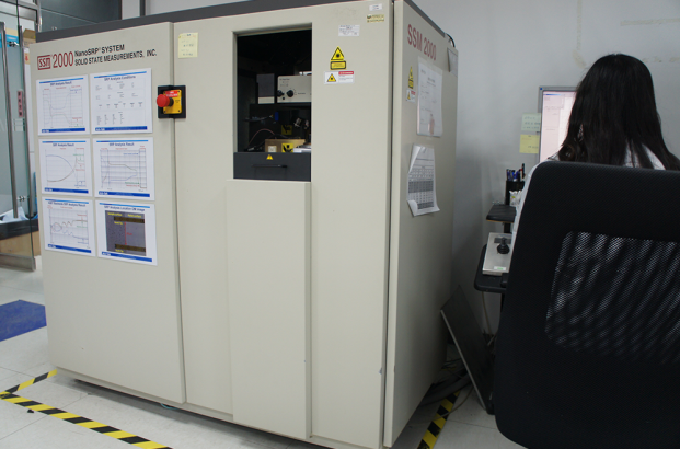
SSM 2000
The resistivity analyzer uses a high-precision probe system and measurement control software to perform point-by-point measurements on the ground surface, establishing the junction depth, resistivity, and effective carrier concentration distribution in semiconductor materials. -
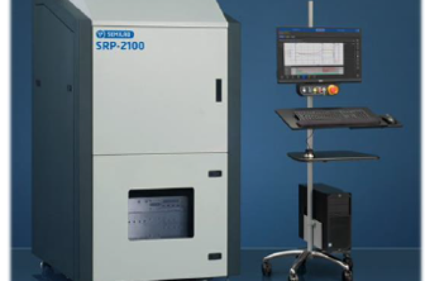
SSM 2100
The resistivity analyzer utilizes high-precision probe systems and measurement control software to perform point-by-point measurements on the ground surface, establishing the junction depth, resistivity, and effective carrier concentration distribution in semiconductor materials.
Application examples
-
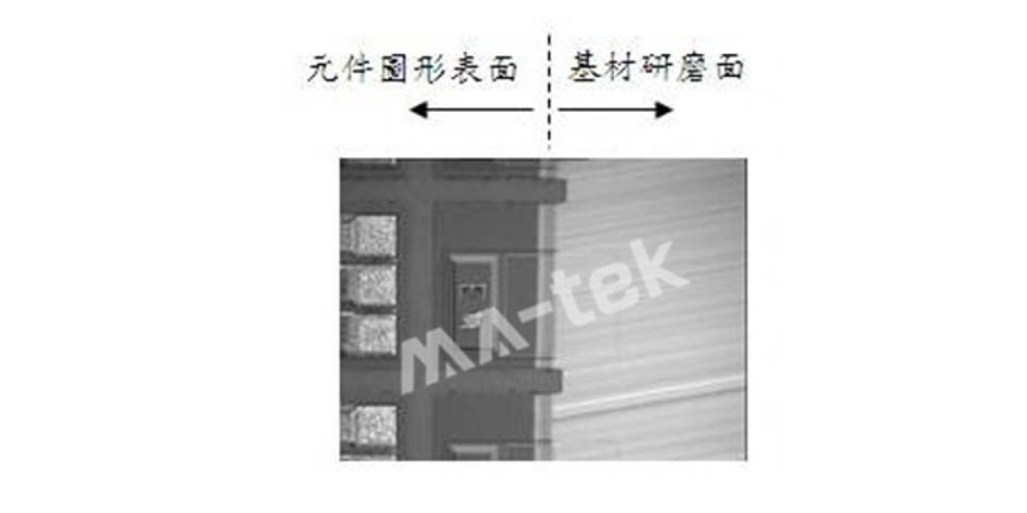
SRP sample grinding surface
The semiconductor sample is ground to form a bevel surface, allowing the component structure and material interface to unfold along the surface. By using a micro-probe of the spreading resistance analyzer to measure resistance values point by point along the ground surface, electrical information at different depths of the material can be obtained. -
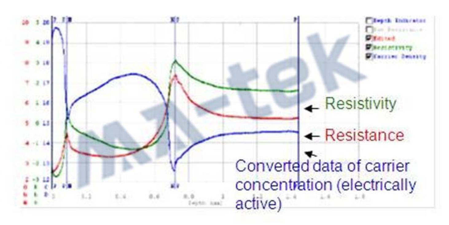
SRP measurement result curve
The measured resistance signal can be converted into the material'sResistivity, Resistance, and Carrier Concentrationdistribution.
By analyzing the curve changes, the semiconductor material can be determined.Doping concentration distribution and Junction Depthused in ion implantation processes and process monitoring analysis.
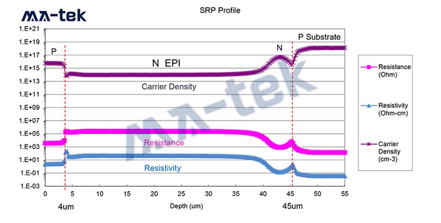
SRP carrier concentration and resistivity depth distribution
This image isThe measurement results of Spreading Resistance Profiling (SRP) analysis.。
The horizontal axis represents material depth (Depth), and the vertical axis represents the electrical parameters obtained from measurements and calculations, including:
-
Carrier Density
-
Resistance
-
Resistivity
It can be clearly identified in the image.P region, N-type epitaxial layer (N EPI) and P-type substrate (P Substrate)the structural differences, and can be judged by the changes in the curveP-N junction position and junction depth。
This analysis technique is commonly used for:
-
semiconductorDoping concentration distribution analysis
-
Junction Depth measurement
-
Epitaxial layer (EPI) quality analysis
-
Ion implantation and annealing process monitoring
Contact
Contact Window
Taiwan Laboratory
Mr. Liu
Shanghai Laboratory


