
InGaAs Gallium Arsenide Indium Micro Light Microscope
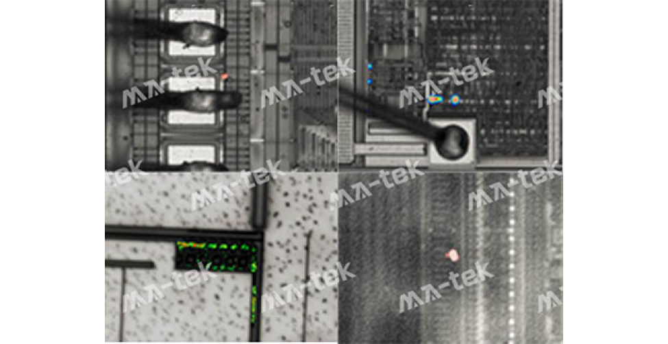
PEM-InGaAs (Photon Emission Microscopy with InGaAs detector)The detection principle is the same as detecting electrons.-Photons emitted from electron-hole recombination and thermal carriers are detected to quickly locate failure positions within the chip by measuring weak photons released during the powered state due to leakage, abnormal conduction, or thermal carrier effects.
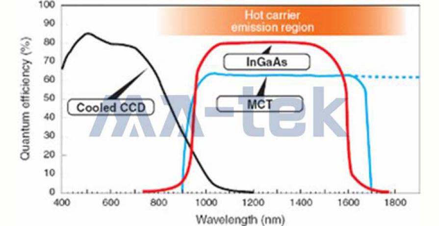
Compared to traditional useSi CCDthe EMMI technology, PEM-InGaAs adoptsInGaAs (Indium Gallium Arsenide) infrared light detectorcan effectively measure900–1700 nmthe near-infrared light range, especially suitable foradvanced processes, low voltage, and low power ICHighlight positioning requirements.
As the semiconductor process nodes continue to shrink, the operating voltage of ICs decreases accordingly, resulting in a decrease in the energy of hot carriers generated during failure, which in turn causes the wavelength of photon emission to gradually shift.infrared segmentIn this trend, the detection capability of traditional CCD EMMI for weak infrared light is gradually limited, whileInGaAs detectors have a smaller bandgap and high infrared quantum efficiency.significantly enhance the sensitivity of hotspot detection, becoming a key technology for advanced process FA. Through PEM-InGaAs, it can quickly locate failure hotspots without damaging the sample, avoiding blind slicing or destructive analysis, greatly improving the efficiency and success rate of failure analysis, making it an indispensable key technology in modern semiconductor FA processes.
-
-
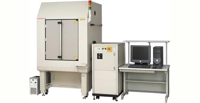 Figure | HAMAMATSU PHEMOS-1000
PEM-InGaAs is particularly suitable for the following analysis needs:
-
Advanced processes and low power IC
-
Low voltage leakage, micro short circuit and soft failure.
-
Backside failure localization requirements
-
Cases where traditional EMMI detection is ineffective
In the failure analysis process, PEM-InGaAs is usually used asThe key first positioning tooleffectively reduce the failure range and connect to subsequent electrical measurements, FIB repair, or structural analysis.
PEM-InGaAs offers multiple key advantages in failure localization applications:
-
High sensitivity infrared detection capability:effectively capture weak leakage and abnormal light signals at low voltage operation
-
Suitable for IC backside analysis:The high infrared penetration through silicon substrates is beneficial for non-destructive localization in advanced processes.
-
Real-time highlight display:Highlights can be displayed in real-time during the measurement period, which helps to quickly adjust measurement conditions.
-
Enhance the success rate of failure localization:It has significant advantages in cases that are difficult to detect with traditional CCD EMMI.
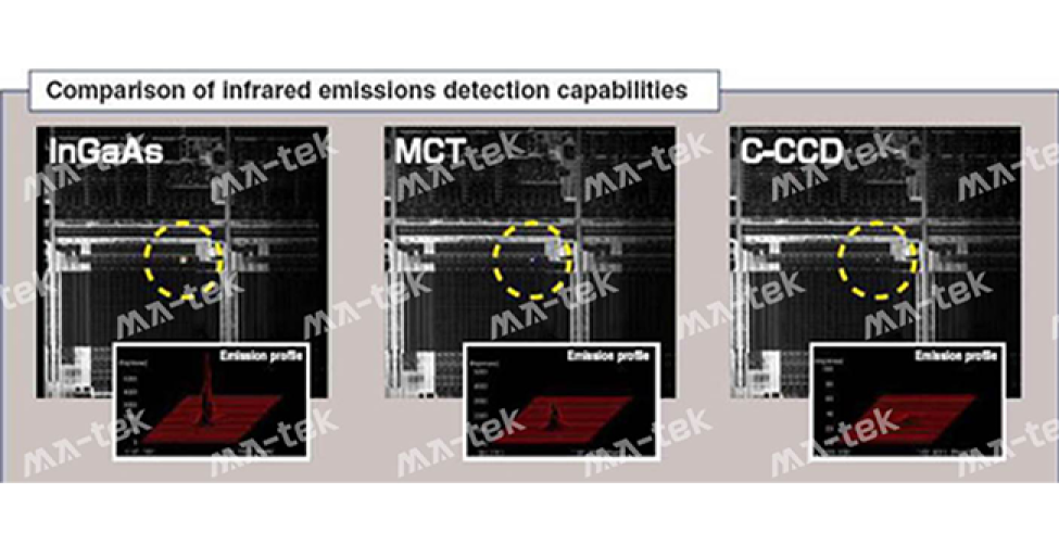
As the processes shrink and operating voltages decrease, the photons released during IC failuresThe wavelength will become longer and enter the infrared range. is The reason why InGaAs can significantly outperform traditional CCD EMMI.:
| Project | PEM-InGaAs | traditional CCD EMMI |
|---|---|---|
| Detection materials | InGaAs | Si CCD |
| detection wavelength | near-infrared (~900–1700 nm) | Visible light to near-infrared (~400–900 nm) |
| low voltage IC | Very suitable | Limited detection capability |
| Advanced Process | Best choice | Insufficient sensitivity |
| backside analysis | high infrared penetration rate | Affected by silicon absorption |


