

IC Packaging and Testing
IC packaging and testing are key stages after the chip has completed wafer manufacturing. The purpose of packaging is not only to protect the chip but also to connect it to the system circuit board and complete the heat dissipation path design with stable electrical and mechanical strength through techniques such as redistribution layer (RDL), wire bonding or bump bonding, and underfill. As the integration and bandwidth requirements of chips increase, packaging is no longer a simple structural operation but a critical link that directly affects signal integrity, thermal management, reliability, and system performance.
In actual processes, factors such as packaging material properties, RDL and bump structures, interlayer thermal expansion differences, soldering and reflow conditions, etc., can cause interface weakening, cracks, metal voids, or electrical shifts. These issues may arise at different stages during the initial packaging, system assembly, and lifespan, thus requiring structural analysis and stress assessment to establish traceable criteria.
MA-tek assists packaging and testing factories in the processes of sample introduction, mass production scaling, packaging conversion, and customer complaint response by providing cross-sectional structure verification, packaging interface integrity analysis, post-packaging electrical change determination, and reliability lifespan assessment. Through high-resolution profile measurement and non-destructive testing, abnormal locations and formation mechanisms can be identified; through reliability testing, the stability of packaging components under temperature cycling, humidity loading, and mechanical stress conditions can be predicted.
Application Examples
Applicable service items
| Service Categories | Common Problem Scenarios | MA-tek provides technology |
|---|---|---|
| Package structure cross-section analysis | Post-packaging electrical anomalies, interface fragility, yield decline | FIB cross-section preparation, SEM / TEM / STEM, EDS material distribution analysis |
| Non-destructive package inspection | Customer complaint cases, packaging consistency confirmation, mass production sampling inspection | X-ray, XCT (3D X-ray), SAM, SAT |
| Packaging stress and thermal behavior assessment | High temperature/reflow anomalies, lifespan degradation | Thermal cycle test cross-section comparison before/after, thermal distribution/stress-related structural analysis |
| Post-packaging reliability verification (RA) | Automotive/Industrial Control/Consumer Electronics Product Life Assessment | TC, HAST, HTS, temperature reflow, Drop Test, Power Cycling |
| Package design/material difference comparison | Risk confirmation during new package introduction or package transfer. | Comparison of structure before and after packaging, analysis of material property differences, design support recommendations |
Application of Multi-Detection Technologies in Packaging and Process Structural Analysis
The figure below shows the application scenarios of different detection and measurement techniques in packaging and process analysis: (a) Optical profilometry (OP) presents the surface height and flatness distribution, used to evaluate structural warpage and morphological differences; (b) Scanning electron microscopy (SEM) observes surface microscopic defects and structural details; (c) Examines the formation and consistency of metal fingers on flexible printed circuit boards (FPC); (d) Conducts photo mask inspection to confirm pattern transfer and process quality. Through cross-comparison of multi-level images and measurement results, effective support can be provided for the interpretation and analysis of packaging structure and process anomalies.
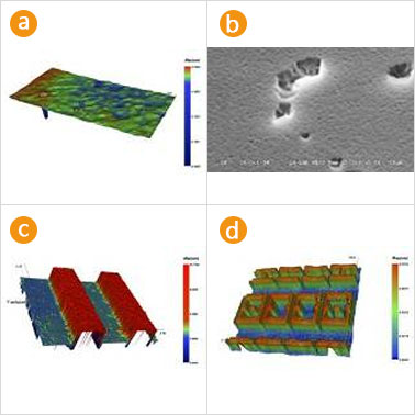
(a) OP;(b) SEM;(c) Metal fingers formation on FPC ;(d) Photo mask inspection
Frequently Asked Questions
Q1. Why does the electrical property of the chip after packaging differ from that before packaging?
A. Thermal load, interface adhesion, and wiring layer stress during the packaging process can affect electrical performance.
Q2. Are there any voids or cracks inside the package, and how can this be confirmed?
A. Such defects may be hidden inside the package and need to be inspected in a non-destructive manner.
Q3. What could be the reasons for failure occurring after a period of time post-packaging?
A. More related to thermal cycling, material fatigue, or interface weakening.
Q4. How to reduce risks when transferring packaging (changing packaging factory/changing packaging materials)?
A. It is necessary to compare the interface, material properties, and electrical differences before and after packaging.
Q5. Can packaging analysis be done with a small sample size?
A. Yes, package cross-section and non-destructive inspection can be completed on a small number of samples.


