
Laser planting ball
In advanced packaging and high-density electronic components, solder balls are not only the core of electrical connections but also directly affect signal transmission stability and packaging reliability. When products enter the stages of research and development verification, failure analysis, or small-scale production, traditional ball placement methods are often limited by process flexibility and precision, making it difficult to meet high density and customization requirements.
Laser re-ballingIt precisely completes the solder ball bonding in a small area through non-contact laser heating and single ball placement control, significantly reducing thermal impact and mechanical stress, becoming an important solution for advanced packaging and analytical applications. MA-tek introduces a high-precision laser ball placement system, providing one-stop services from R&D sample production, packaging rework to electrical verification, assisting customers in quickly establishing testable samples and improving development efficiency.
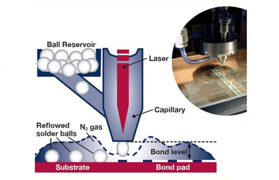
Principle diagram of laser ball placement technology
The solder balls are delivered by nitrogen and precisely bonded to the solder pads through localized heating by lasers, achieving high-quality bonding with low thermal impact.
Compared to traditional processes, it has obvious advantages: the ball planting process does not require flux, nor does it need subsequent cleaning, and it can effectively avoid material deformation and structural stress caused by overall heating.
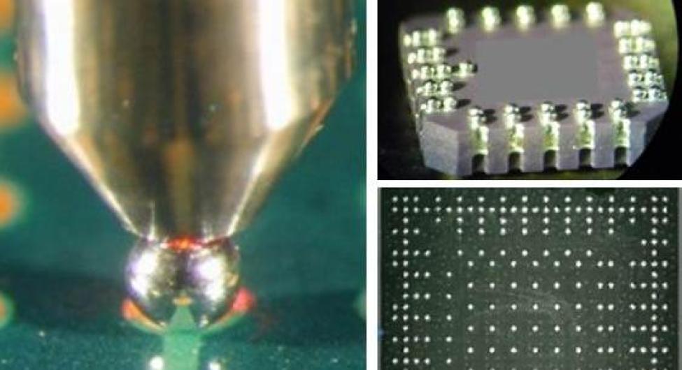
Laser ball placement actual application images (BGA / micro-pitch solder balls)
It can accurately complete single ball placement on high-density solder pads, suitable for fine pitch and high-density packaging. In addition, the ball placement layout can be preset, and no additional fixtures are required during the process, effectively enhancing operational flexibility and process efficiency.
Laser ball planting technology can be applied in various fields of semiconductors and electronic products, including BGA, CSP, Flip-chip, and wafer bumping packaging processes. It is also suitable for 3D packaging, optoelectronics, MEMS, and high-precision applications such as camera modules. In practice, it is often used in PCB adapter board development, small batch sample production, and the repair and rework of BGA-type packaging, making it particularly suitable for electrical verification and troubleshooting during the research and development phase.
Under the trend of high density and high complexity in packaging, laser ball placement has become a key role in connection technology. MA-tek, through high-precision equipment and rich process experience, not only provides stable and reliable ball placement quality but also seamlessly integrates with material analysis, failure analysis, and reliability testing. This means that customers can not only "complete ball placement" but also complete verification, analysis, and problem resolution on the same platform, significantly shortening the product development cycle and improving the success rate. Laser ball placement ensures that every solder ball "lands in the right position," and MA-tek ensures that they are not only in place but also in place and reliable.
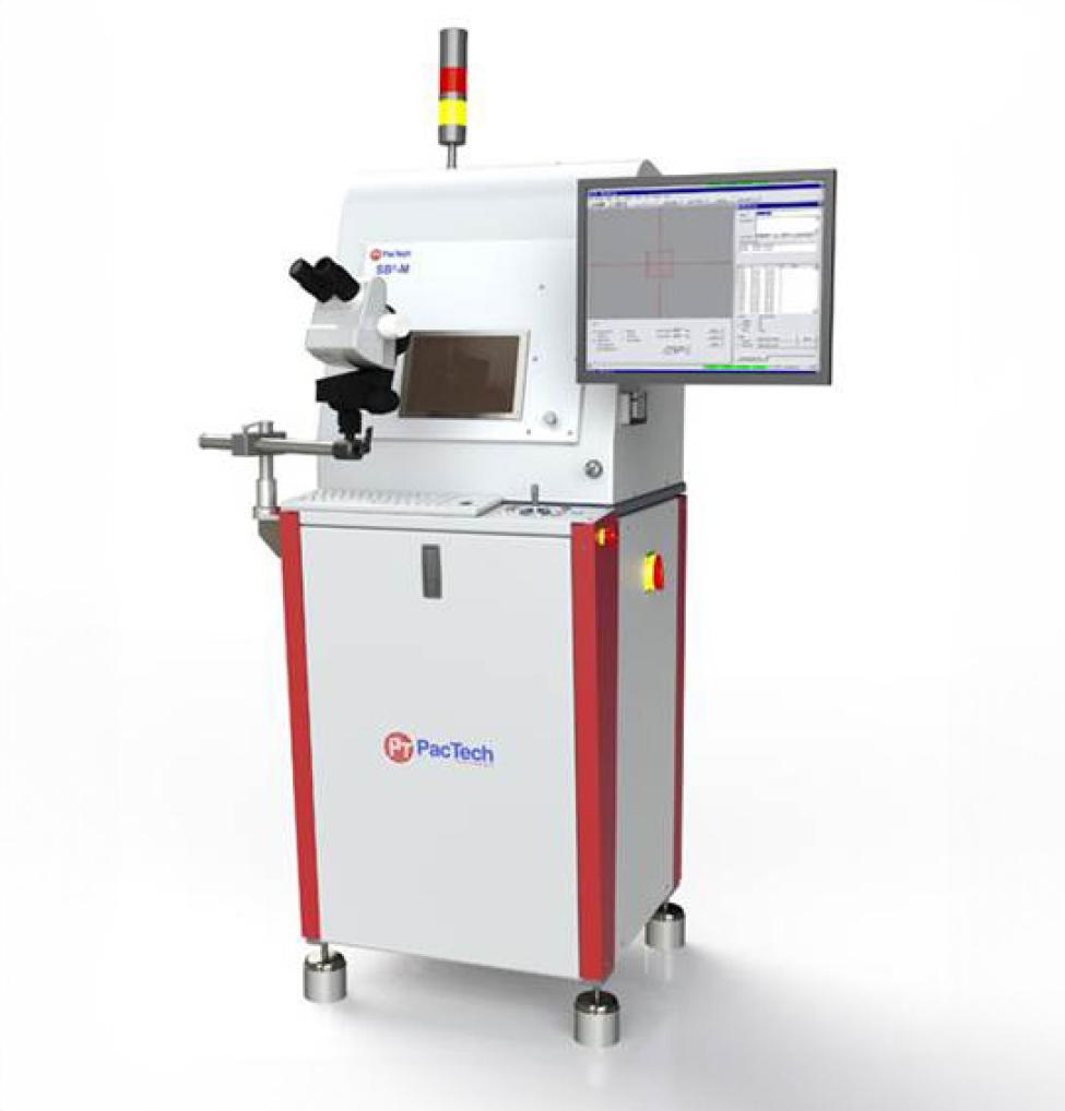
High-Precision Laser Ball Placement Equipment (PacTech SB2-M)
The equipment can achieve a ball placement speed of up to approximately 5 solder balls per second and supports a ball diameter range of 100 μm to 350 μm, balancing efficiency and application flexibility.
MA-tek's laser ball placement service integrates ball placement and reflow functions, allowing for solder ball bonding without the need for additional reflow processes, significantly simplifying the process flow. Through automatic calibration and imaging monitoring systems, consistency in the position and quality of each solder ball can be ensured. The system supports various solder compositions, including SnPb, High-lead, SnAg, and SnAgCu, and has good eutectic bonding capability to meet different application needs. In addition, the equipment supports tray operation and 2D/3D imaging monitoring, effectively enhancing process stability and traceability.


