
SAT ultrasonic scanning microscope
Scanning Acoustic Tomography (SAT)also known asSAM (Scanning Acoustic Microscope)It detects abnormalities such as delamination, voids, or cracks at various interface layers within advanced packaging by utilizing the imaging characteristics of ultrasonic reflection rates and return energy differences in materials of different densities, and by selecting different frequency probes. In the fields of electronic packaging, semiconductors, thermal conductive materials, resin composites, and module reliability analysis, SAT is one of the most important interface inspection tools, particularly suitable for detecting "internal defects" that are difficult to identify with the naked eye and optical microscopes.
SAT uses ultrasonic frequencies above 20 kHz, while semiconductor-grade probes typically range from 15 to 230 MHz; the higher the frequency, the better the resolution, but the penetration depth decreases. Therefore, probes need to be professionally selected based on packaging thickness, resin type, and structural material. The medium for SAT is "pure water" as the sound wave transmission medium, which can effectively enhance acoustic coupling, allowing ultrasound to enter the interior of resin, silicon, metal, or multilayer packaging with minimal loss, receiving the signal.(Acoustic impedance signal)converted into A-scan(waveform)、C-scan(image)、B-scan(image)、S-Image(HitachiMachine image diagram)、3Dimage..., etc.
The imaging basis of SAT comes from the changes in reflection, scattering, and penetration of ultrasound as it transmits through different materials. Its operating principle includes the following three core mechanisms:
- Ultrasonic transmission and acoustic impedance differences:The core principle of SAT comes from the difference in "acoustic impedance". When ultrasound transmits from a water medium into different materials such as silicon grains, metals, resins, air, adhesives, and ceramics, each material has a different acoustic impedance, resulting in different reflection intensities. The greater the difference in acoustic impedance (for example: resin vs. air), the stronger the reflection. Therefore, SAT is particularly sensitive to "voids, delaminations, and cracks."
- Depth Profiling:After the ultrasonic wave is emitted, different echo signals will be generated according to the density and elasticity of the material interfaces. By calculating the time delay (Time of Flight), reflection intensity (Amplitude), and scattering pattern (Scattering Profile), the interfaces at different depths inside the package can be reconstructed into a three-dimensional image. Through continuous depth scanning, the bonding status between the resin, grains, solder, and packaging structure can be inspected layer by layer.
- High-frequency ultrasound and resolution:The SAT probe frequency generally covers 15–230 MHz. Low frequency has stronger penetration, suitable for thick packaging; high frequency has higher resolution and can identify small interface anomalies.SAT can detect encapsulated molded packages with a thickness greater than 4 mm.It can also identify subtle delamination structures in advanced packaging, suitable for large BGA, QFN, and Power modules.
SAT ultrasonic scanning microscope is commonly used to detect various hidden defects inside the packaging, such as delamination, voids, cracks, breakage, uneven resin, and bonding anomalies, especially those interface issues that are difficult to capture with X-ray or optical methods. As IC packaging develops towards thinner, larger, multi-layer stacking, and composite integration, SAT has become the standard analytical tool for verifying encapsulation quality, die attachment, interface integrity, and multi-layer structure reliability.
In packaging structure analysis, SAT can clearly identify issues such as package crack, delamination, die crack, void in resin, poor contact in filled holes, and uneven die attach with high-contrast imaging. Its high sensitivity is sufficient to reveal air gaps in extremely thin dielectric layers and tiny voids in metal filled holes, and it can assess the interface condition in resin packaging after lead-free solder ball reflow.
In power modules, power components, and ceramic composite packaging, SAT is irreplaceable for the detection of metal/ceramic interfaces, thermal interface materials, and silver adhesive bonding. Ultrasound can penetrate resin, ceramics, and multilayer materials, presenting internal interface variations with high sensitivity, providing important basis for process improvement, packaging optimization, and reliability analysis.
1.Package Crack:Can detect cracks in molding compound, epoxy resin, or the packaging perimeter caused by thermal or mechanical stress, and can track the direction and depth of crack propagation.
2.Interlayer delamination and delamination:It can identify local delamination at the interfaces between molding and substrate, DAF and die, underfill and RDL, which are key indicators of packaging reliability failure.
3.Voids in Resin:It can assess the voids caused by bubbles, moisture, or uneven material mixing in molding packaging, underfill filling, or die attach, which have a significant impact on subsequent thermal cycling reliability.
4.Die Crack:The ability to observe cracks caused by stress at the grain boundaries or within the grains is one of the important aspects of chip reliability analysis.
5.Die Attach quality assessment:It can determine the spreading and adhesion status of silver paste (Ag epoxy), DAF film, and Solder Die Attach, which are essential verification items for power modules and high-power packaging.
6.Metal filled holes (Via / Plated Hole) poor contact:Can identify incomplete metal-filled holes in TSV, ReVia, or PCB vias, such as voids inside the holes, inclusions, or uneven filling density.
MA-tek has two advanced SAT devices, Hitachi FS300II and Sonoscan GEN6, which can meet the multilayer interface analysis needs from general packaging, BGA, QFN to high power modules, MEMS, and advanced materials.
-
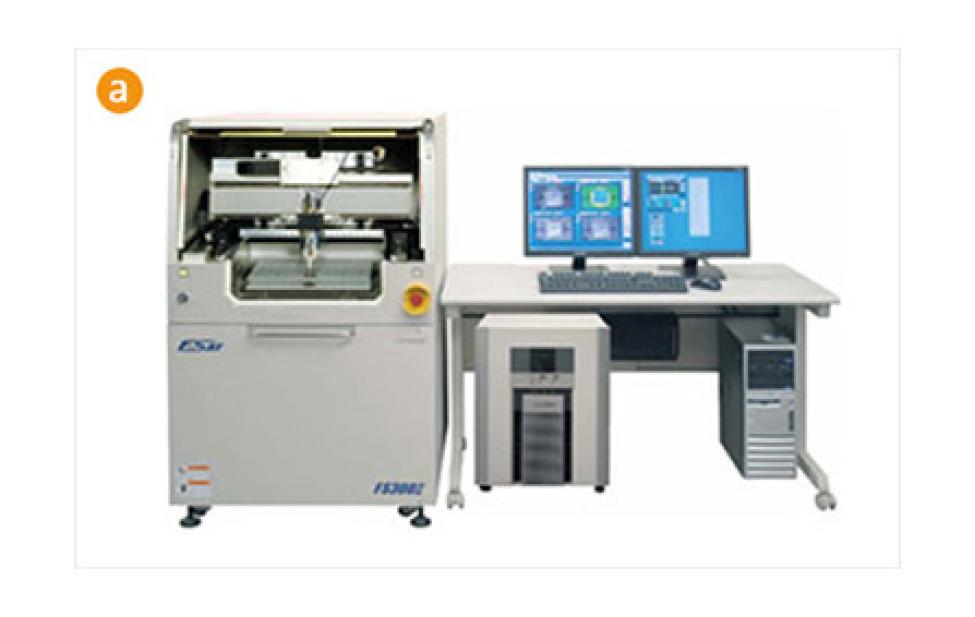
Figure | Hitachi FS300II
-
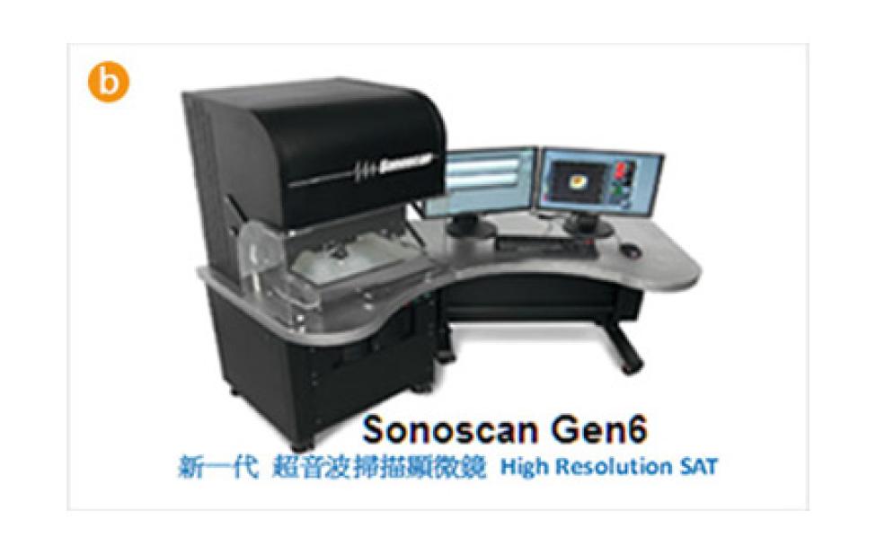
Figure | Sonoscan GEN6
- High bandwidth probes (15–230 MHz):The probe frequency ranges from 15 to 230 MHz, allowing for the selection of different probes based on material characteristics, packaging thickness, and structural requirements to optimize the balance between penetration and resolution. High-frequency probes can identify extremely fine interface defects, while low-frequency probes can detect thicker packages or products with more material layers, achieving the best balance between imaging penetration depth and resolution.
ultrasonic frequency Characteristics Scope of Application 15–30 MHz strong penetration Thick packaging, resin body, power module 30–100 MHz Balance between resolution and penetration power Most IC packages / PCBs 100–230 MHz High resolution, able to discern fine defects WLP, MEMS, Microelectronics - High-speed scanning (up to 1000 mm/s):The high-speed scanning capability supports the inspection of a large number of samples, improving the efficiency of quality control for mass production. At the same time, it maintains positioning accuracy, making the interpretation of internal defects in packaging more reliable.
- High depth resolution (0.5 μm):MA-tek's SAT system has a high resolution of 0.5 μm, allowing for precise differentiation of differences between adjacent layer interfaces, such as uneven adhesion of DAF (Die Attach Film), Underfill cracks, and tiny voids within encapsulant resin.
- Multi-mode imaging capability:SAT has multiple scanning modes that allow the same sample to be fully analyzed from different angles. Through multi-mode integration, engineers can quickly interpret defect depth, interface anomaly locations, and subsequent quality conditions, significantly improving problem localization efficiency. At the same time, they can choose the most suitable measurement method based on material characteristics and defect types, ensuring that the analysis results are more accurate and reliable.
Scanning mode Characteristics A-scan (single point waveform scan) Display the echo time and intensity at a single location, providing interface depth and reflection characteristic data. B-scan (Profile Scan) The side view cross-section presented along the linear direction clearly indicates the depth of the defect location on the Z-axis. C-scan (planar scan) Presenting the 2D defect distribution at a specific depth is the most commonly used mode for package quality inspection. S-image (multi-layer image overlay) Integrate images of different depths for analyzing the differences in multilayer interfaces of packaging structures. T-scan (transmission scan) Receiving sound waves from the other side is suitable for checking the overall material transmittance and large area defects. 3D Acoustic Imaging Integrate multi-layer scanning results into a three-dimensional structure for visualizing crack orientation, delamination extent, and internal geometric properties of materials.
-
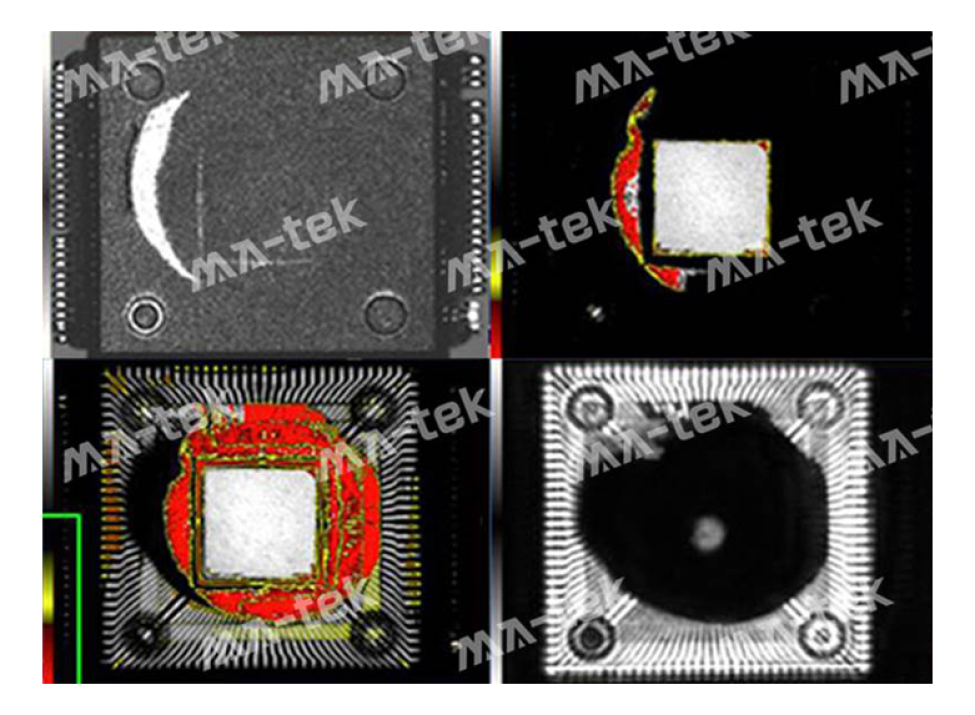
The SAT C-scan image shows delamination inside the package and die attach anomalies.
In the upper left and upper right images, obvious high-reflection areas can be observed at the grain boundaries and the interface of the packaging material, indicating delamination or poor adhesion at the interface. The upper right image enhances the defect range through grayscale, clearly identifying the location and distribution of abnormal areas. The image below shows the scanning results of the complete packaging structure, where the red areas represent locations with strong acoustic reflections, usually corresponding to voids, delamination, or interface separation phenomena.
-
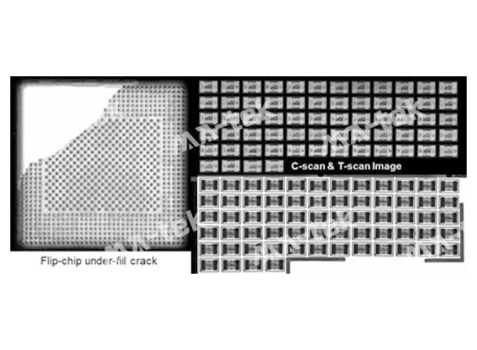
Image | SAT applied to various electronic packaging defect detection cases
Typical applications of SAT in different electronic components include package cracks, MLCC component defects, flip-chip packaging voids, and poor adhesion of heat sinks. Due to the different acoustic impedance characteristics of various material interfaces, significant echo differences occur when ultrasonic scanning reaches the interface, resulting in high contrast images of cracks, voids, or delamination areas inside the package.
-
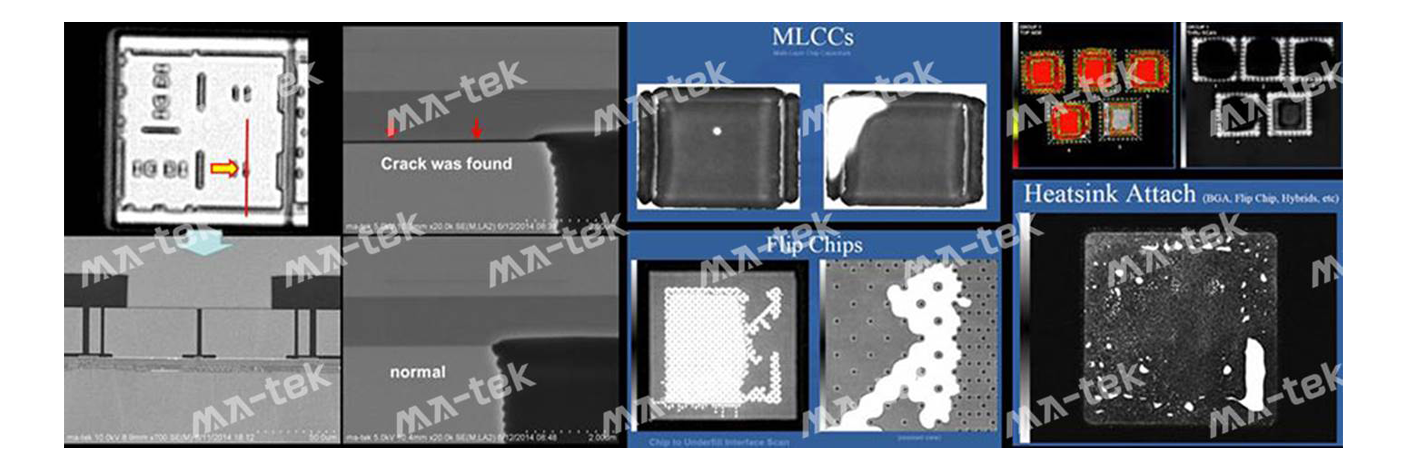
Figure | Typical case of SAT ultrasonic scanning microscope in semiconductor packaging defect detection
Various SAT C-scan image examples, including package cracks, chip attachment interface anomalies, MLCC component defects, flip-chip voids, and poor adhesion of heat sinks. Due to different acoustic impedances at different material interfaces, significant reflection contrasts are formed during ultrasonic scanning, allowing for clear identification of defect locations such as delaminations, cracks, and voids within the package.
-
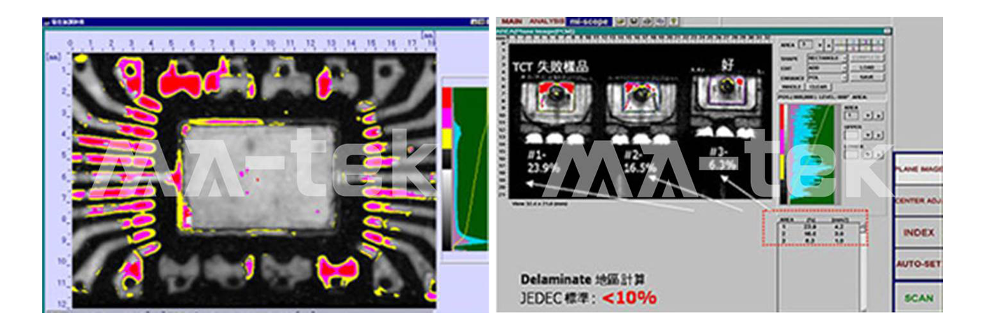
Image | Quantitative analysis of package delamination in SAT C-scan
SAT images can be analyzed for defect area statistics through software, marking the delamination areas of the package interface with colors and calculating the ratio. The example in the image shows the interface delamination conditions of different samples after thermal cycling tests (TCT), and judgments are made according to JEDEC packaging reliability standards. Through SAT's high-resolution scanning and image analysis, the delamination ratio inside the package can be quickly quantified, assessing packaging reliability and process quality.


