
Fault Analysis and Solution Process
In the development and mass production of semiconductors and electronic products, any anomalies or failures can affect product yield, reliability, and market competitiveness. The core value of Failure Analysis (FA) lies in accurately identifying failure mechanisms and root causes through systematic processes and diverse analytical techniques, thereby assisting customers in proposing effective improvement measures.
MA-tek combines years of material analysis and failure analysis experience to establish a complete and standardized failure analysis process, from initial information gathering, non-destructive testing, to electrical localization and physical analysis, providing a one-stop and highly efficient analysis solution to assist customers in quickly clarifying issues and shortening product development and verification timelines.
From sample reception, data confirmation to multi-stage analysis and final report, a complete and traceable analysis process is established. When customers submit abnormal samples, background information collection and problem definition will first be conducted, including usage conditions, process information, and failure phenomena. If the information is insufficient, further confirmation of key parameters will be made with the customer to ensure the correctness of the analysis direction. After that, it enters the analysis planning stage, where the most suitable analysis strategy is formulated based on product characteristics and failure modes.
The first step of the analysis process usually employs non-destructive analysis techniques to avoid irreversible damage to the samples while quickly narrowing down the problem scope. By using methods such as optical microscopy (OM), ultrasonic scanning (SAT), X-ray, electrical measurements (I-V), and thermal imaging (Thermal EMMI), the internal structure of the package, solder joint conditions, and potential abnormal areas can be observed. The purpose of this stage is to establish a preliminary judgment of the failure location and serve as an important basis for subsequent in-depth analysis.
When non-destructive analysis confirms the presence of anomalies, it will further proceed to Electrical Failure Analysis (EFA). In this stage, various electrical measurement and localization techniques, such as EMMI, OBIRCH, InGaAs, EBIC, or Nanoprobing, can accurately locate abnormal points such as leakage, short circuits, or open circuits within the chip. The key to electrical analysis lies in converting "invisible electrical problems" into "observable spatial locations," providing clear targets for subsequent physical analysis.
After completing the electrical localization, the abnormal area will be further analyzed through Physical Failure Analysis (PFA). This stage often uses techniques such as delayering, scanning electron microscopy (SEM), energy dispersive spectroscopy (EDS), and FIB cross-section analysis to directly observe material structures, defect morphologies, and process anomalies. Through high-resolution imaging and elemental analysis, failure phenomena such as metal fractures, contamination, voids, and interface delamination can be confirmed, and the failure mechanisms can be gradually established.
When a deeper understanding of material properties and chemical states is needed, advanced material analysis (Material Analysis, MA) techniques such as SIMS, TEM, SCM, and other high-level analytical tools will be further introduced. This stage can analyze element distribution, chemical bonding, and nanoscale structures, ultimately completing root cause identification. Through cross-scale analysis, it establishes a correlation between failure phenomena and process conditions or material properties, providing specific and feasible improvement directions.
After completing the analysis of each stage, MA-tek will provide a complete preliminary report and final analysis report, which includes explanations of failure location, failure mechanism, and root cause. At the same time, based on the analysis results, we can assist clients in proposing improvement suggestions and preventive measures (Corrective Action & Prevention). If the cause of failure is related to the usage environment, reliability testing can also be conducted to further verify the failure mechanism and product tolerance.
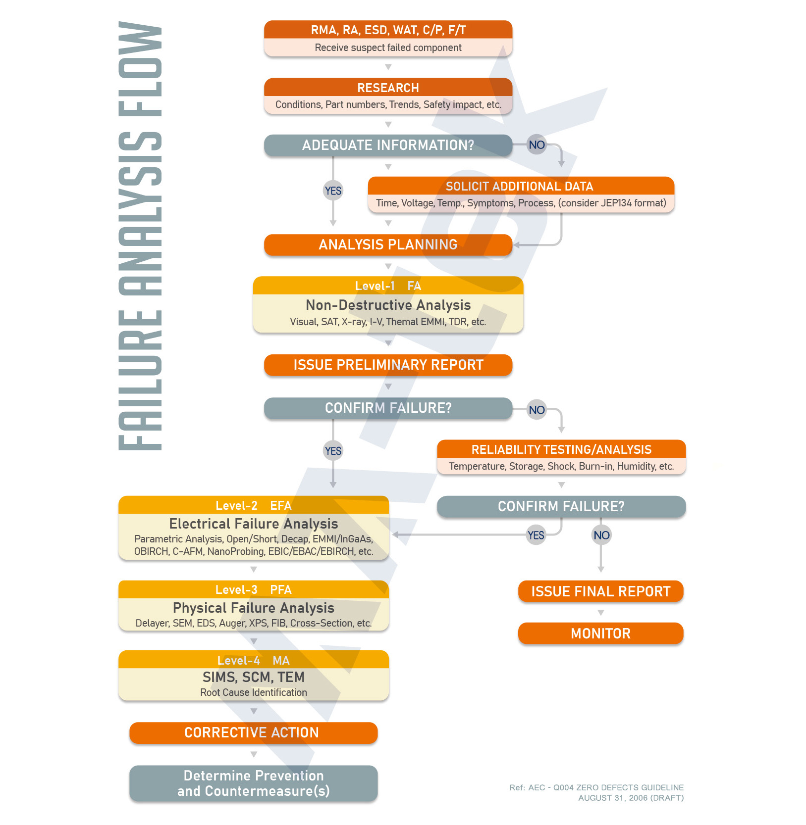
Diagram | Failure Analysis Flow


