
FIB circuit repair
FIB utilizes gallium as an ion source, using the negative electric field applied to the extractor to pull gallium atoms from the tip, forming a gallium ion beam. The ion beam is focused through an electric lens, and the size of the ion beam can be determined by a series of aperture changes, finally focusing the ion beam onto the surface of the sample. Because gallium atoms are located in the middle of the periodic table, the removal effect caused by using them to collide with other elemental atoms is far greater than that of electrons, allowing for specific pattern processing on the surface of the sample using the ion beam.
General SB-FIB can provide functions such as material cutting, metal deposition, metal etching, and selective etching of oxide layers to meet the needs of circuit repair. With the help of gas-assisted etching systems, it can not only improve the etching selectivity and etching rates of different materials but also directly deposit specific materials. Currently, the auxiliary etching gases of MA-tek's SB-FIB machines can be applied to enhance the etching rates of polymers, metals (Al & Cu), and oxides. The types of auxiliary deposition gases include platinum (Pt), tungsten (W), and tetraethyl orthosilicate (TEOS). If SB-FIB is combined with a field emission scanning electron microscope (i.e., Dual Beam FIB, DB-FIB), real-time cross-sectional observation can be performed.
What is FIB circuit editing?
FIB circuit repair, also known as circuit edit, is commonly abbreviated as FIB. It is a type of instrument developed for modifying layouts on ICs. FIB machines have many functions, including localized cross-section observation and TEM sample preparation for structural or failure analysis. To avoid confusion, it is still recommended to specify that circuit repair is to be performed when commissioning, rather than just saying FIB. The type of machine used for circuit repair belongs to single beam, which means using an ion beam for ion impact to remove surface material as a tool for circuit cutting. If circuit connections are to be made, a metal layer, such as tungsten, must be deposited to connect two or more metal lines. At this time, it is also necessary to use W(CO)6 gas, which, after being decomposed by the Ga+ ion beam, can achieve tungsten deposition. MA-tek currently has 15 Single Beam FIB (SB-FIB) microscopes available to provide IC circuit repair services, meeting diverse customer needs for product failure analysis, along with professional technical support and experienced personnel to provide accurate, precise, efficient, and effective rapid product failure analysis services.
Although FIB and scanning electron microscopy (SEM) and transmission electron microscopy (TEM) were invented around the same time in the 1950s, FIB was used in research and development fields until 1993 when it began to be applied in IC product failure analysis, especially in the technology industry for targeted cutting of specific defect sample locations to provide sample preparation for SEM and TEM, etc. IfCombined with gas-assisted etching systems, it is more widely applied in semiconductor integrated circuit line repairs, saving a significant amount of product debugging time and shortening the time for changing photomasks.
MA-tek offers a variety of FIB machines (SB/DB) for selection, assisting our customers in enjoying more efficient and effective services.To provide the best service quality and a diverse range of services, MA-tek continues to invest in purchasing many of the latest instruments and equipment every year. The services include metal layer cutting for IC circuit repair, wire bonding and probing pad production, precision cutting of tin whiskers in lead-free processes, reliability failure cross-section analysis of tin-lead solder joints, complete observation of copper process cross-sectional structures, as well as providing analysis services for many more advanced IC process technologies.
- Precision Cutting
- TEM Sample Preparation
- IC Circuit Editing and Verification
- Abnormal Process Analysis
- Ion Channeling Contrast for Grain Morphology Observation
- GDS Auto-Navigation to Designated Failure Address
- Passive Voltage Contrast Analysis for Fault Isolation
In the IC design and manufacturing process, products that have undergone tape-out need to undergo functional verification to confirm whether they meet testing standards. However, there are often performance differences and even functional defects. At this point, design debugging is necessary to identify the issues and revise the design for re-production. This entire process forms a loop; the faster the problems are identified, the quicker the product can be brought to market (time to market). As products become increasingly complex, the time taken to revise the photomask and proceed to manufacturing until a finished product is available is very time-consuming. If the time for design debugging can be saved, it can shorten the overall time from engineering to mass production. There are many methods for design debugging, including testing, simulation, failure analysis, and circuit repair. The engineering team spends considerable effort confirming the issues to ensure that the next revised product can achieve the expected performance. Among these methods, circuit repair is utilized by almost all R&D engineers. By modifying the circuit, the need to redo the photomask and the R&D costs of initial prototypes can be eliminated. This operational model is definitely effective in shortening the time from R&D to mass production while also saving a significant amount of R&D expenses, making the customer's products more timely and competitive in development.
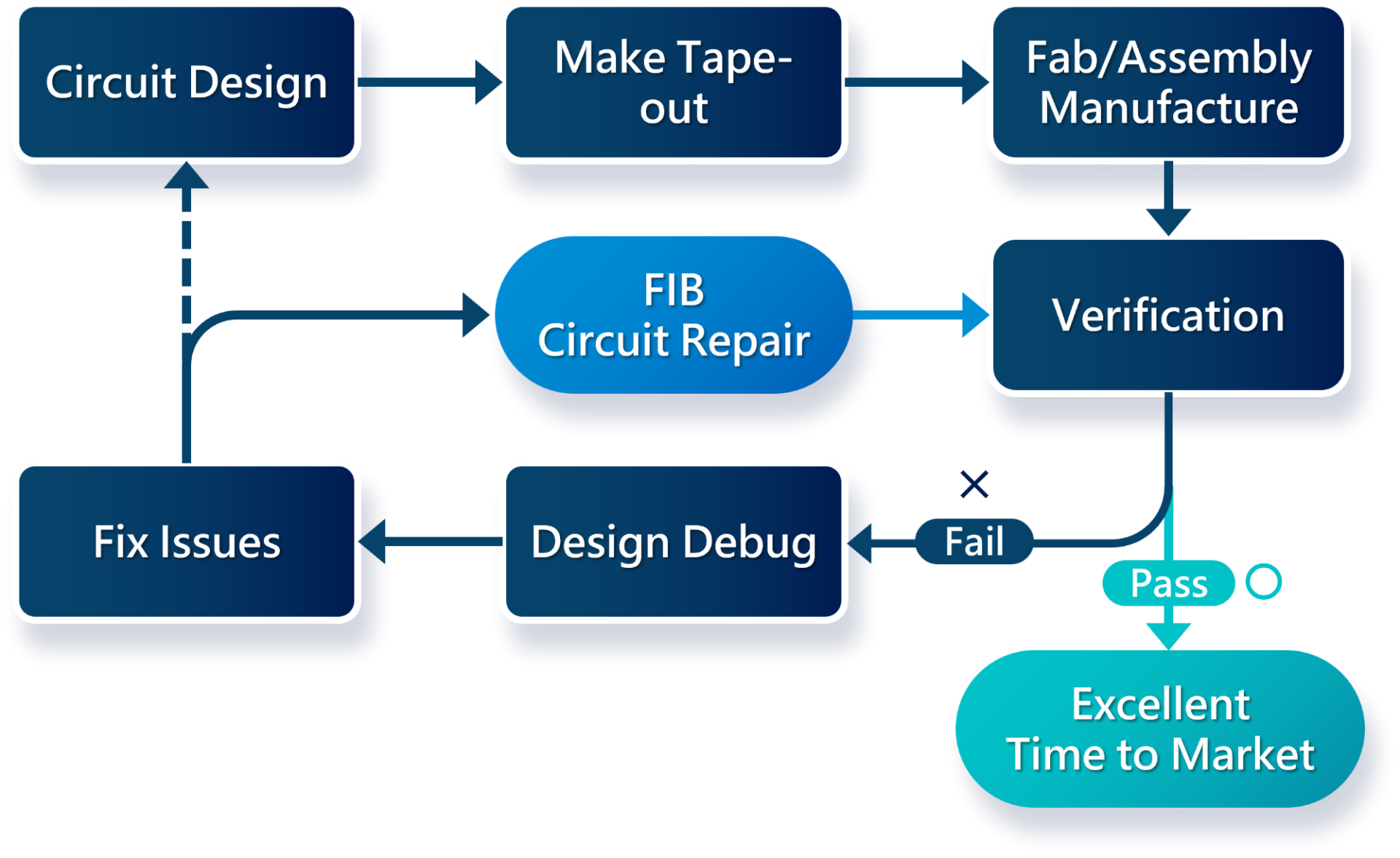 Figure 1 shows the flowchart from circuit design, product manufacturing, verification, identifying design issues to revision. The faster the problems are solved, the shorter the time to market, gaining a competitive advantage.
The process of circuit repair will first involve internal discussions on the client side to identify the necessary modifications, after which a proposal and process will be provided. The proposal includes the planar locations and metal layers where circuit cutting and connections need to be made, and it will be determined whether the client needs to provide GDS files based on the situation. Generally, if the circuit cannot be clearly identified from the surface of the sample, GDS is needed for automatic navigation to the correct position to reduce the failure rate of execution (Figure 2). Considering cybersecurity risks, regional GDS files can be provided (Figure 3). After the sample is completed, if there are no further requirements, the executing unit will delete the files. Once the executing unit receives the request, it needs to discuss and evaluate the case with the commissioning client, providing the required man-hours and proposal yield. If necessary, the proposal can be revised to improve the success rate of the implementation. After both parties confirm that there are no issues, it will enter the execution schedule, and upon completion, it will be sent back to the client for testing to verify whether the proposal was successful.
-
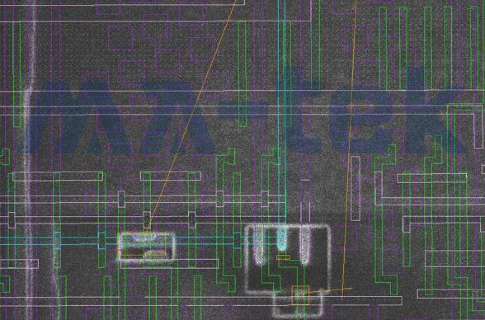
After aligning the GDS layout in Figure 2 with the sample surface, the correct position for circuit repair is found using coordinates.
-
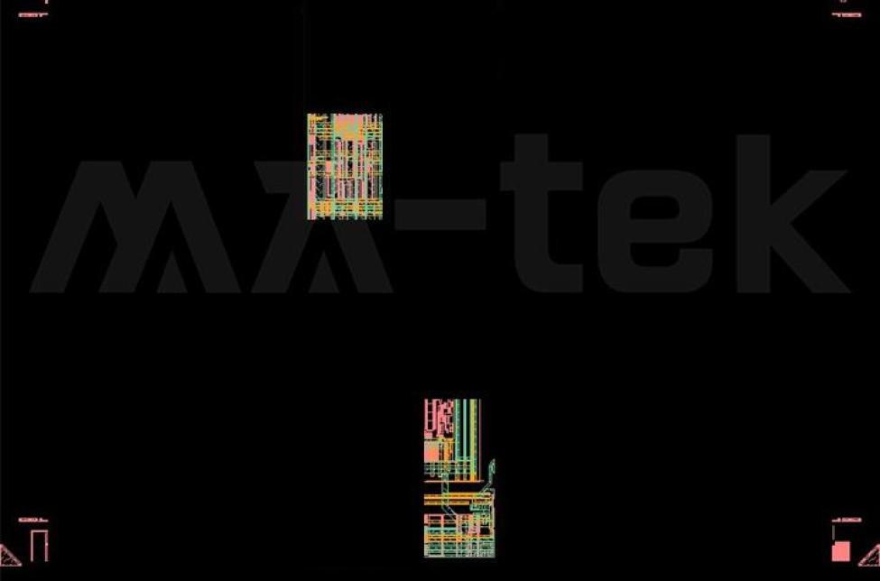
Figure 3 The GDS provided by the customer must include the positions of the four corners for calibration, as well as the GDS for the location and layers of the circuit repair work, without disclosing customer confidential information.
The time and yield required for the circuit repair process will vary depending on the sample's manufacturing process, the difficulty of the solution, and the completeness of the sample information. The methods and techniques used must be adjusted in real-time according to the current execution situation. Therefore, it relies not only on advanced instruments and devices but also on engineers with considerable experience to face and resolve various unexpected situations, thereby achieving the results expected by the customer.
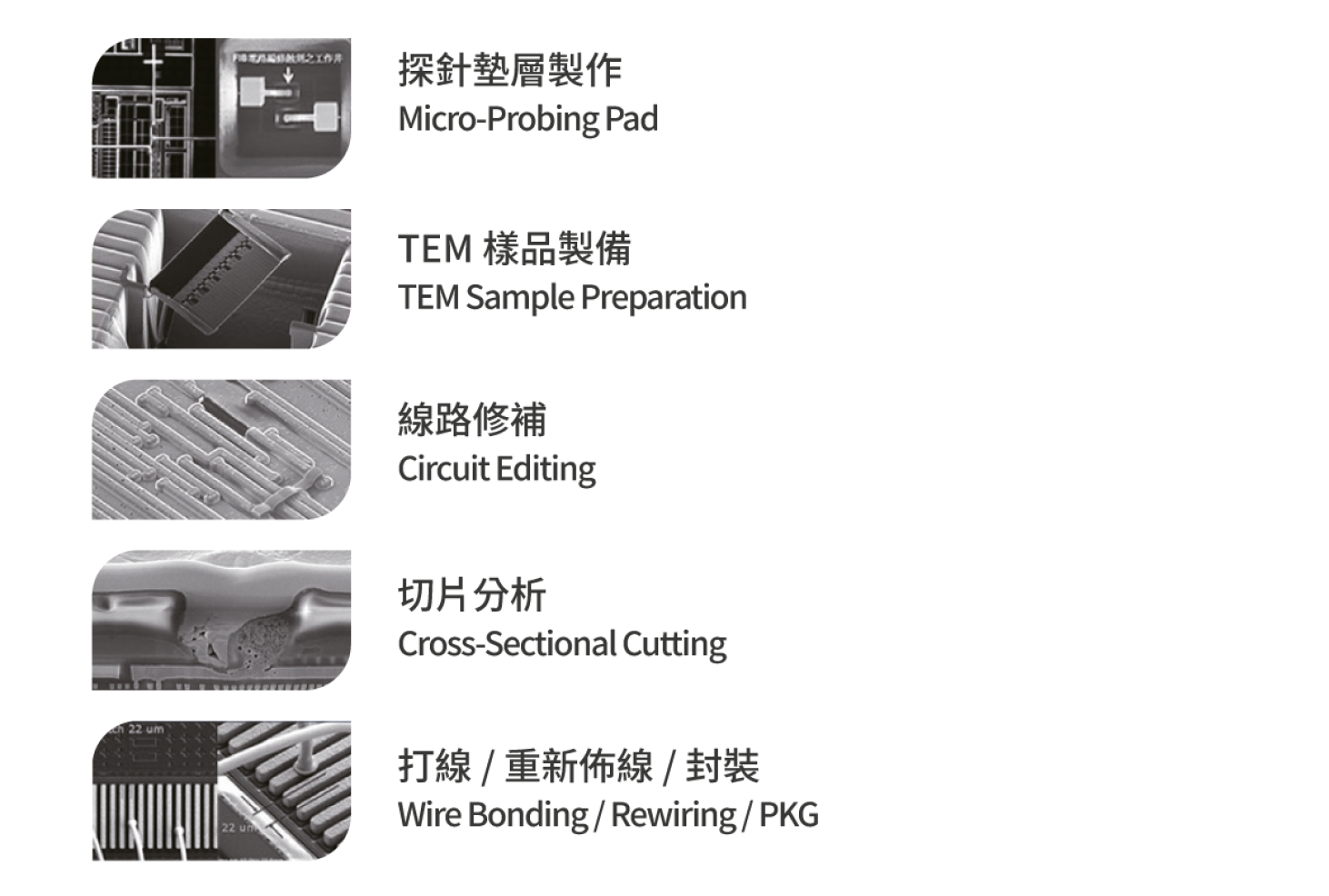
Available options include services such as metal layer cutting, wire bonding and probe pad layer fabrication, precision cutting of warping in lead-free processes, failure analysis of tin-lead bump cross-sections, cross-sectional structure observation, and advanced IC process technology analysis services.
-
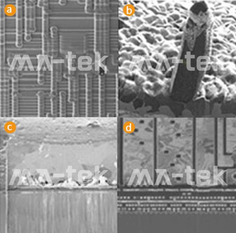
(a) FIB IC circuit modification
(b) Precision cutting of tin whiskers (Sn Whisker) in lead-free processes
(c) Pb-Sn Solder Ball reliability failure cross-section precision cutting
(d) Observation of cross-sectional structure of copper process cutting at high tilt angles
-
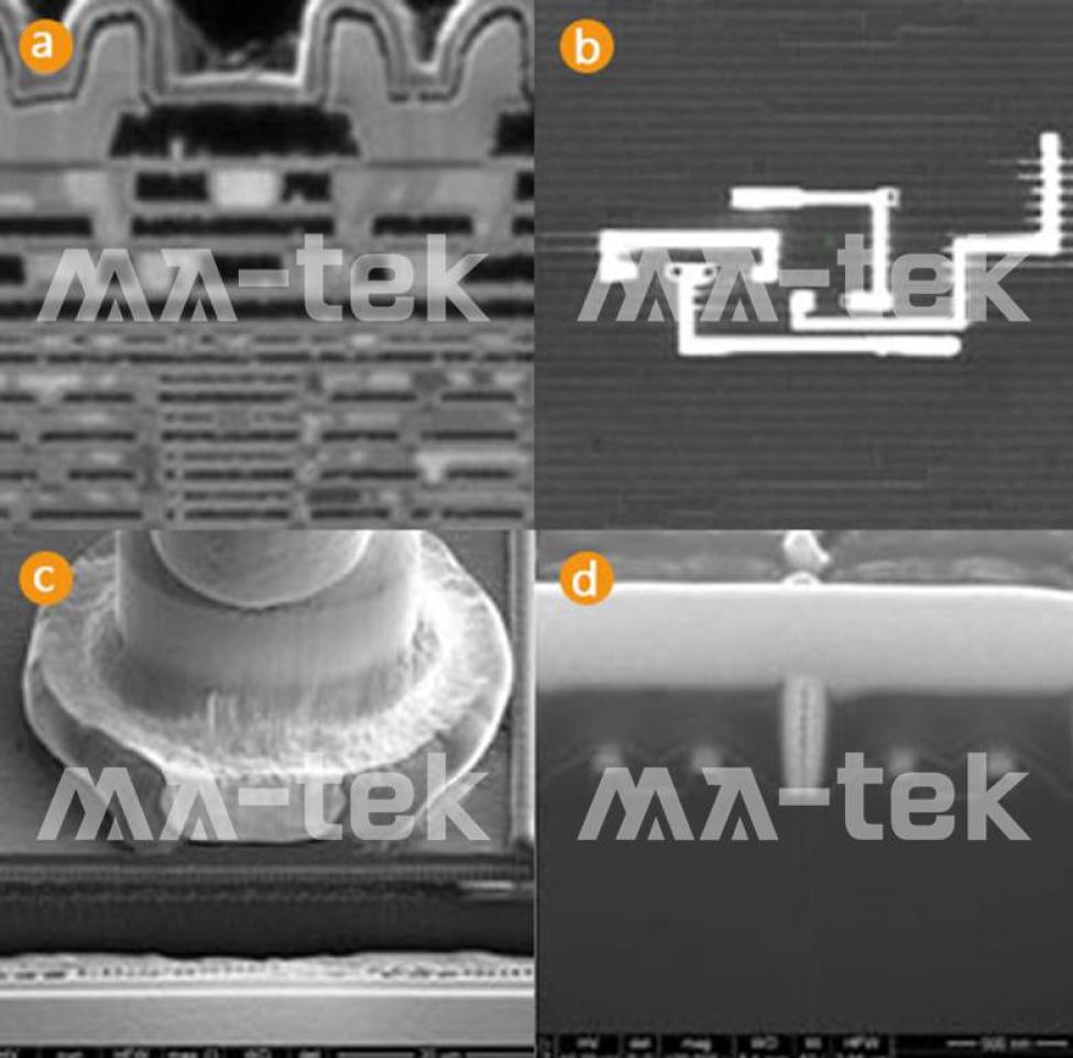
(a) Complete cross-sectional structural observation of the copper process
(b) FIB IC circuit modification
(c) Large area cross-sectional structure observation of gold wire ball bonding
(d) Process anomaly analysis observation
-
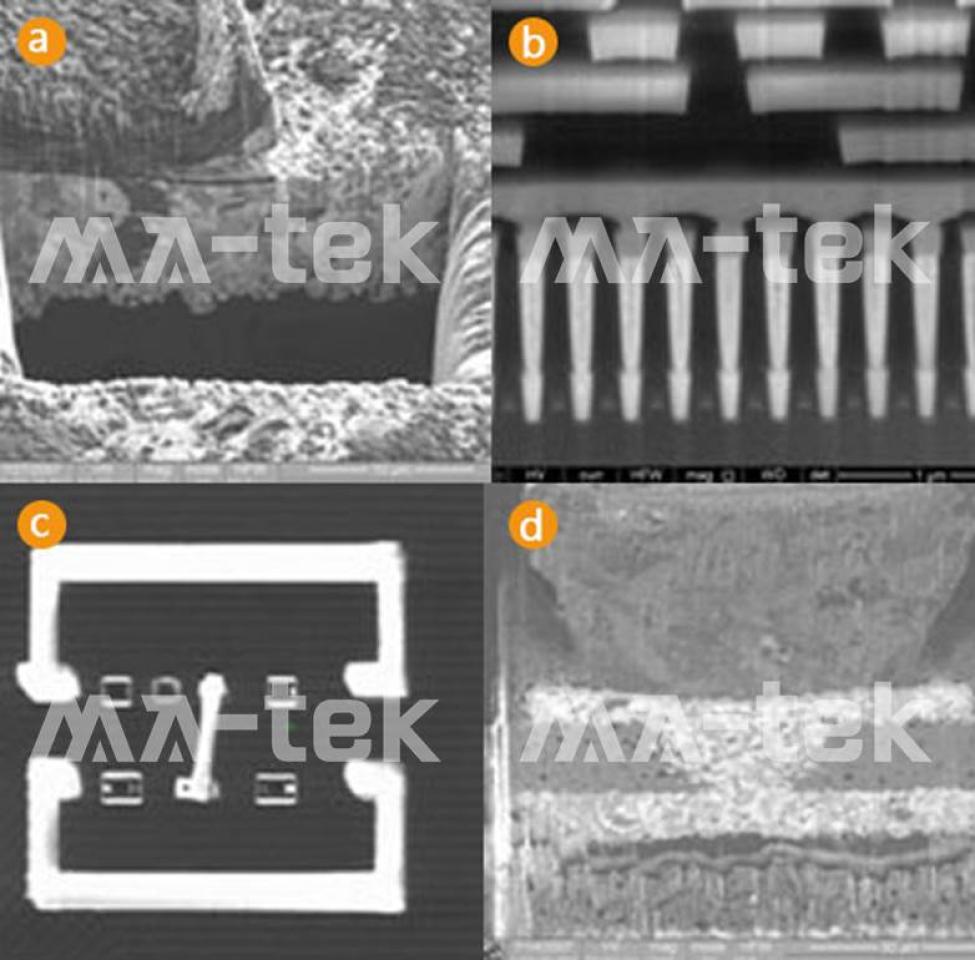
(a) Grain analysis observation
(b) Cross-sectional structure observation
(c) FIB IC circuit modification
(d) Cross-sectional structure observation of copper wire vias in printed circuit boards (PCBs)
-
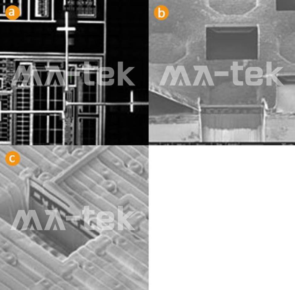
(a) Fabrication of uncoated cross test pads
(b) Large area cross-sectional structure observation
(c) Cross-sectional observation after circuit repair


