
EBIRCH electron beam induced resistance change technology
EBIRCH (Electron Beam Induced Resistance Change) electron beam induced resistance change technologyIt is an electrical localization method conducted in a scanning electron microscopy (SEM) environment. Through the resistance changes caused by the localized heating effect of the electron beam, EBIRCH can detect areas of abnormal resistance in circuits and precisely locate defect positions within the metal interconnects, poly, or contact layers of ICs.
EBIRCH technology is often applied to:
-
IC short circuit (Short defect) localization
-
High-resistance metal interconnect defects
-
Abnormal conduction in metal/via/poly layers
-
Failure analysis of nanoscale process interconnects
-
Failure Localization
EBIRCH analysis must be conducted in a SEM chamber environment. During measurement, engineers use two nano-probes to contact the PAD or metal wires (Metal / Via) on the chip, forming a current loop and applying DC bias. As the electron beam scans the surface of the sample, the energy of the electron beam causes slight temperature changes in the localized material. Since the resistance of conductors and semiconductors changes with temperature, localized resistance variations occur near the area illuminated by the electron beam, leading to changes in the current signal. By detecting the location of the current signal variations, abnormal areas in the circuit can be pinpointed in the EBIRCH image. This technique is particularly effective for analyzing metal short circuits or localized resistance anomalies, enabling rapid identification of failure locations at the nanoscale.
Compared to traditional optical laser positioning techniques (such as OBIRCH), EBIRCH has higher spatial resolution. Since EBIRCH locates defects using electron beam scanning in a SEM environment, its resolution can reach the nanoscale, making the bright spots more concentrated and the positioning more precise. In practical applications, the size of the bright spots generated by EBIRCH is usually smaller than100 nm²The highlight of the optical system's OBIRCH may be greater than750 nm²Therefore, in advanced process IC analysis, EBIRCH can more accurately locate abnormal areas, making it particularly suitable for nanoscale metal interconnect defect analysis. In addition, the EBAC technology mainly targets open issues, while when the defects belong to short circuits or high-resistance anomalies, EBIRCH is often a more effective analysis tool.
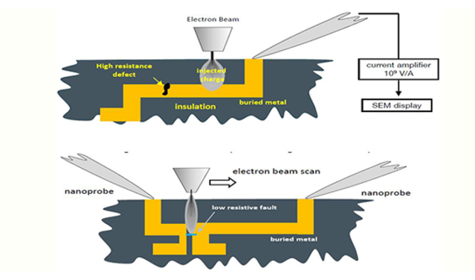
Schematic diagram of the principles of EBAC and EBIRCH technologies
EBAC mainly locates open circuit defects in metal interconnects by exciting the absorbed current in the metal wires with an electron beam; whereas EBIRCH utilizes localized temperature increases caused by electron beam irradiation to change the material's resistance, leading to current changes. By measuring the variations in current signals, the locations of short circuits or high-resistance defects can be identified. Both techniques have complementary roles in semiconductor failure analysis, enhancing the efficiency and accuracy of defect localization.
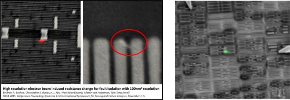
Figure 2 successfully locates the position of the short using EBIRCH.
By Brett A. Buchea, Christopher S. Butler, H. J. Ryu, Wen-hsien Chuang, Martin von Haartman, Tom Tong [Intel], ISTFA 2015: Conference Proceedings from the 41st International Symposium for Testing and Failure Analysis, November 1–5,
In advanced process IC failure analysis, a single analysis technique often struggles to fully locate defects. Different types of defects, such asOpen, Short, Leakage, or High Resistanceneeds to be combined with different electrical localization techniques for cross-validation.
MA-tekThrough integrationEBIC, EBAC, EBIRCH and OBIRCHAdvanced positioning technologies can quickly identify defect locations for different failure modes, and further confirm the root cause by combining with physical analysis methods such as FIB and TEM.
As the process nodes advance towards5nm, 3nm, and even 2nmThe internal structure of the chip has become more complex, and defect locations are often found in deep metal layers or at the nanoscale junctions.
Through the cross-application of different analysis techniques, it is possible to:
-
Increase defect localization success rate
-
reduce misjudgment
-
shorten analysis time
-
Improve the success rate of subsequent FIB/TEM sample preparation
Therefore, in advanced process failure analysis,EBIC, EBAC, EBIRCH and OBIRCHhas become an indispensable electrical localization tool.
| Analysis technology | Main Principle | Applicable defect types | Application |
|---|---|---|---|
| EBIC | The electron beam generates electron-hole pairs and forms a current image. | Junction leakage、Gate oxide breakdown | Interface defect localization, oxide layer breakdown analysis |
| EBAC | Electron beam excites the metal wire current and tracks the conduction path. | Metal open、High resistance | Multi-layer metal interconnect open circuit localization |
| EBIRCH | The electron beam causes localized temperature rise leading to resistance changes. | Metal short、High impedance | Metal short circuit and high impedance defects |
| OBIRCH | Laser localized heating causes resistance changes. | Short defect、Leakage path | Packaging and chip short circuit localization |


