TFT-LCD industry
Common issues in the TFT-LCD industry include bright and dark spots, line defects, Mura (uneven brightness), material contamination, metal diffusion, abnormal film thickness, and interface delamination. These problems often require the integration of material analysis, surface analysis, and failure analysis techniques to accurately locate the source of defects and clarify the failure mechanism.
MA-tek combines material analysis (MA), surface analysis (SA), and failure analysis (FA) to provide a complete TFT-LCD inspection and analysis solution. Through techniques such as optical microscopy (OM), scanning electron microscopy (SEM), energy dispersive spectroscopy (EDS), focused ion beam (FIB), X-ray, surface profile measurement, and various chemical analyses, it can deeply analyze panel structure, thin film material composition, and micro-defect distribution, assisting customers in quickly locating process abnormalities and improving product reliability and mass production yield.
TFT-LCD manufacturing defect analysis cases
In the TFT-LCD display panel manufacturing process, factors such as film deposition, etching, mask alignment, and material quality can all affect the integrity of the TFT structure and the electrical performance of the components. Through material analysis and high-resolution structural observation techniques, precise localization of process defects and determination of failure mechanisms can be conducted. The following are common analysis cases in the TFT-LCD manufacturing process.
1. Particle contamination causing dark spots
In the TFT-LCD manufacturing process, if there is particulate contamination in the process environment or on the material surface, it may cause local structural abnormalities in the TFT components, thereby affecting the normal operation of the pixel circuits and leading to dark spot defects on the display panel.
Through Optical microscopy (OM) planar observationcan quickly locate defect areas, and then useCross-section SEMConducting structural analysis can further confirm the impact of particle contamination on metal layers or dielectric layers and determine the cause of defect formation.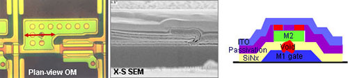
2. Residual metal from Source/Drain etching
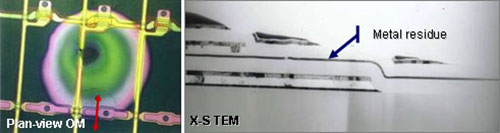
In the TFT device manufacturing process, if the Source/Drain metal etching does not completely remove the material, it may leave metal residues in the device structure. These residues may cause:
-
Electrical leakage
-
Short circuit risk
-
Component reliability decline
throughOptical Microscope (OM)Surface anomalies can be observed, and then utilized.transmission electron microscopy (TEM)Conducting high-resolution structural analysis can clearly identify the location and morphology of metal residues, further clarifying the reasons for etching process anomalies.
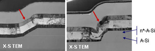
3. Sidewall angle analysis of a-Si layers
in TFT-LCDamorphous silicon (a-Si) thin film structureis an important key affecting the electrical properties of the components. When the sidewall angle or morphology control between the n⁺-aSi and intrinsic a-Si layers is poor, it may affect:
-
Component channel characteristics
-
Current transmission efficiency
-
Component stability
Through Cross-section TEM analysisThe structural profile and interface morphology of the a-Si layer can be clearly observed, and the film deposition and etching processes can be evaluated to see if they meet design requirements.