
TEM sample preparation
In transmission electron microscopy (TEM) analysis, samples must be prepared asUltra-thin samples (usually less than about 100 nm)to ensure that the electron beam can smoothly penetrate the sample and form high-resolution images, for the analysis of semiconductor components or materials cross-sections, it is often utilizedFocused Ion Beam (FIB)For precise sampling and thinning of specimens, in FIB cross-section TEM specimen preparation,The methods includePre-ThinLift-out,Omni-probe,Different preparation methods have their own advantages and disadvantages, and the choice usually depends onsample characteristics, analysis requirements, and time costs。
Transmission Electron Microscope,TEMis a high-resolution analytical technique capable of observing structures at the nano or even atomic scale. However, whether TEM can obtain high-quality images and accurate analytical results,Greatly depends on the quality of sample preparation.。
The basic principle of TEM analysis is to use a high-energy electron beam to penetrate the sample to form an image, so the sample must be prepared toExtremely thin samples (usually less than 100 nm)to allow the electron beam to penetrate smoothly. If the specimen is too thick, the electron beam will not be able to effectively penetrate the sample, resulting in a significant decrease in image resolution, or even failing to form an effective image. In addition to the thickness requirement, the preparation of TEM specimens must also take into account the following important conditions:
-
The thickness of the specimen is uniform.to avoid image contrast distortion
-
Avoid mechanical damage and stress deformation
-
Maintain the original microstructure of the sample
-
Precise positioning analysis area
In the analysis of semiconductor devices or advanced materials, TEM often needs to observe specific nanostructures, such asgate oxide layer, metal interconnect, interface structure or defect location,Therefore, the preparation of TEM samples not only needs to achieve a sufficiently thin thickness, but also must be able toPrecise sampling of target areas,As semiconductor processes continue to shrink, traditional mechanical grinding methods have struggled to accurately locate analysis areas at the nanoscale, thereforeFocused Ion Beam (FIB)has become an important tool for TEM sample preparation. Through the nanoscale processing capability of FIB, precise cutting and thinning can be performed at designated locations to produce high-quality samples suitable for TEM observation.
Since FIB has nanoscale processing capabilities, it can perform precise cutting and thinning at designated locations, thus enabling operations at the micrometer or even nanoscale.Accurately obtain the target area TEM sampleCompared to traditional mechanical grinding preparation methods, FIB not only improves sample positioning accuracy but also significantly reduces structural damage caused during the sample preparation process, making it particularly suitable foradvanced semiconductor processes, nanomaterials, and complex multilayer structuresIn the analysis of FIB cross-sectional TEM sample preparation, the three common methods include:
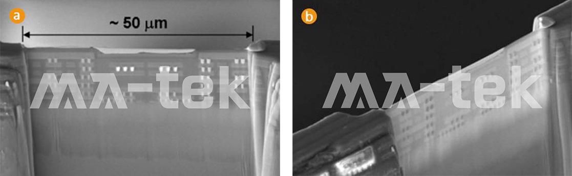
Pre-Thinning is a method that combinesMechanical grinding and FIB thinningthe TEM sample preparation method. First, use mechanical grinding to reduce the sample thickness to about5–10 μmthen further thinned to a thickness suitable for TEM observation (about0.1 μm), the main advantage is that it can prepareLarge area and uniform thickness TEM thin region (approximately 50 μm)Since the thin area is still supported by the original material, the specimen is not easily damaged.Deformation or curlingthe problem, which is beneficial for high-quality TEM imaging observation. However, the pre-thinning method requires going throughGrinding and FIB two process stepsThe overall production process is relatively complex and time-consuming. In addition, there is still a risk of sample damage or grinding failure during the mechanical grinding process, which requires higher demands on operating techniques and equipment conditions.
The electrostatic attraction method is commonly used.FIB in-situ sampling technologyUsing FIB to thin the target area, and then throughU-shaped cuttingSeparate the thin slice from the original sample. Then use a glass probe toElectrostatic attraction methodTaking out the thin slice and placing it on a copper grid with a carbon film, the greatest advantage is thatFast production speed and high efficiencyThe preparation time for a single sample is usually controllable within1 hourTherefore, when a large number of TEM samples need to be analyzed, this method is often used. However, once the samples are placed on the carbon film copper grid, further processing or adjustments cannot be made. Therefore, the control of sample thickness and quality usually relies onExperience judgment of FIB engineers。
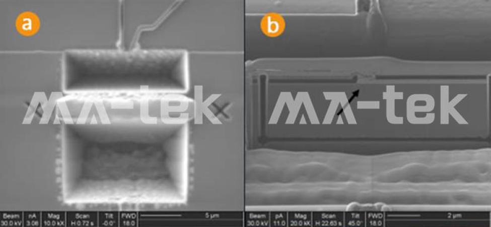
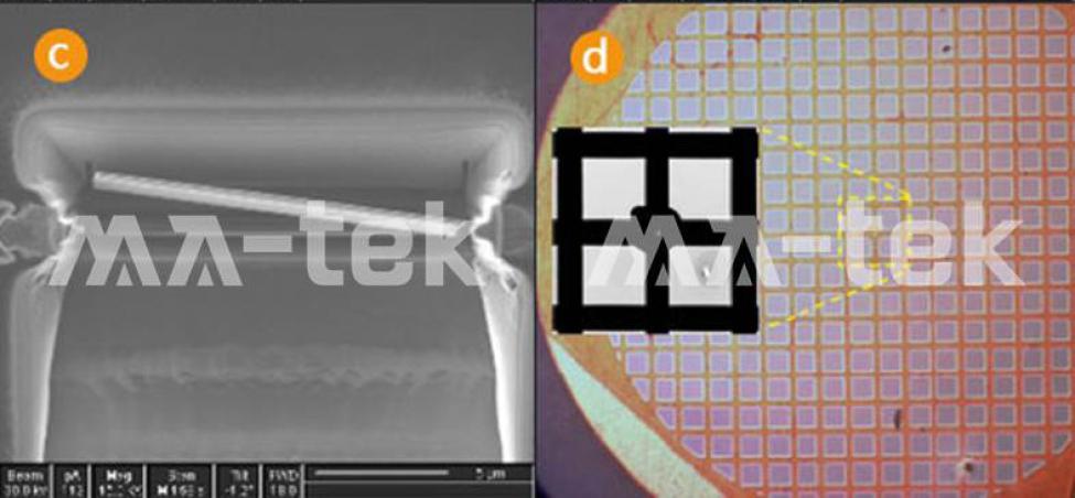
The lift-out method (Omni-probe) is a more precise TEM sample preparation method, which first uses FIB to roughly cut the target area toapproximately 1–2 μm thicknessand partially separated from the sample, then deposited through FIBPlatinum (Pt)The microprobe is welded to the sample, and then the sample is moved to the TEM sample holder (TEM grid). After fixing the sample, the probe is cut off using FIB, and further processing of the sample is carried out.final thinninguntil the thickness required for TEM observation is reached.
This method, although it isThe most complex and time-consuming TEM sample preparation method.The overall preparation time is about1.5 to 2 hoursbut its greatest advantage is that the sample canRepeatedly entering and exiting FIB for adjustments or reprocessing.Therefore, for the analysis of high-value or critical samples, this method is often adopted to ensure the quality of the specimen and the reliability of the analysis.
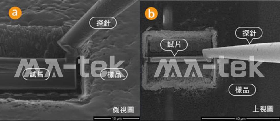
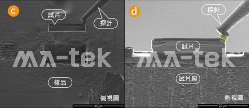
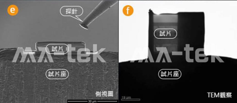
Through the steps, TEM samples with suitable thickness for electron beam penetration can be prepared for high-resolution structural and material analysis.
(a) Attach the probe to the completed cut specimen
(b) Using FIB to deposit Pt to fix the probe and the sample.
(c) Lift the sample out of the original specimen
(d) Fix the sample to the TEM sample holder (TEM grid)
(e) Cut off the connection between the probe and the sample.
(f) Place the sample into the TEM for observation and analysis.


