
Spherical aberration corrected scanning transmission electron microscope (Cs-STEM)
Advanced processes require detection and analysis at the sub-angstrom scale (1 Å = 0.1 nm).
Currently, the world's leading chip manufacturers are actively advancing the mass production of process technologies below 2 nanometers (nm) and are targeting process nodes at the angstrom (1Å = 0.1nm) scale. As the size of transistors shrinks, traditional silicon-based materials also face physical limits, prompting the industry to explore new materials such as 2D materials (like graphene and transition metal dichalcogenides), nanowires, GAA (Gate-All-Around), nanosheets, and stacked heterostructures to break through the bottleneck of Moore's Law. However, when device sizes enter the sub-angstrom scale, details such as the atomic arrangement within the material, interface defects, and doping distribution can have a significant impact on device performance. Therefore, accurately analyzing the structure and composition of materials at the angstrom scale has become an important issue in the development of semiconductor technology.
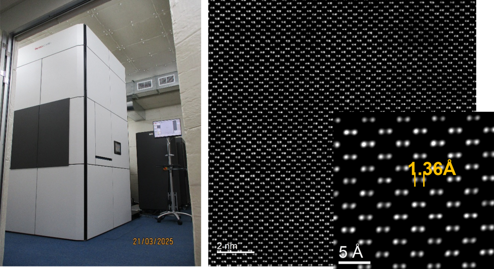
The Spherical Aberration Corrected Scanning Transmission Electron Microscope (Cs-STEM) is an analytical tool responding to advancements in new materials. Using a spherical aberration corrected TEM can improve the spatial resolution of the machine, achieving observation at sub-angstrom dimensions. TEM combined with scanning functionality is referred to as the Scanning Transmission Electron Microscope (STEM). STEM, along with Energy-Dispersive X-ray Spectroscopy (EDS) and EELS, can achieve high spatial resolution compositional analysis.
* 1 micrometer (μm) = 1000 nanometers (nm) = 10000 angstroms (Å)


