
Delayer dry etching and grinding to remove layers
Dry etching and delayering (Delayer) is throughIon dry etching, chemical etching or mechanical grindingIn this way, the metal layers and dielectric layers inside the integrated circuit (IC) are removed layer by layer, allowing for clear observation and analysis of each layer's circuit structure. Modern semiconductor chips typically contain multiple layers of metal interconnections, such as Metal1, Metal2 to Metal6, and even more layers. These metal layers and oxide layers are stacked on top of each other to form a complex circuit architecture, therefore during the process ofDefect localization, process diagnosis or circuit analysisAt times, it is often necessary to use layer removal technology to sequentially remove materials to reveal the wiring structure of each layer.
In the delayering process, engineers must precisely control the material removal rate and stop layer position to avoid damaging the underlying circuits or destroying critical structures. By using appropriate etching conditions and grinding processes, they can stay at specific layers and preserve target structures, allowing for subsequent microscopic analysis and circuit observation. Through the chip structure after delayering, engineers can combine.Optical Microscope (OM) and Scanning Electron Microscope (SEM)To conduct high-resolution observations and further confirm process defects or analyze circuit designs, dry etching and mechanical polishing delayering techniques are widely used in semiconductor process defect analysis, IC open/short circuit fault localization, detection of metal layer cracks and etching residues, analysis of circuit wiring structures, and IC reverse engineering.
IC layer removal mainly utilizesChemical etching, gas dry etching, or mechanical grindingthe method, gradually removing the metal layers and dielectric layers in the internal structure of the chip. By precisely controlling the etching conditions or grinding rate, it is possible to stop at specific layers and retain the target structure for subsequent analysis. In practical analysis, engineers usually willCombining multiple layer removal techniquesto ensure that each layer of the circuit structure can be clearly presented and avoid damage.
-
Chemical etching layer removal:Use acidic or alkaline chemical solutions to selectively dissolve metal or oxide layers.
-
Reactive Ion Etching (RIE):Materials are removed through plasma reactions and ion bombardment, allowing for precise control of etching directionality and uniformity.
-
Mechanical Polishing:Using precision grinding equipment to gradually grind away materials is suitable for quickly removing large area layers.
In the process of semiconductor failure analysis and product dissection, IC delayering technology effectively assists engineers in locating the source of defects and analyzing circuit designs by removing materials layer by layer and observing the structure of each layer.Failure Analysis ApplicationsIn the process, layer removal technology can be used to observe possible anomalies that may occur, such as: metal layer disconnections or cracks, poor via filling, etch residue, oxide layer defects, metal short circuits or open circuits. By analyzing the circuit structure layer by layer, it is possible to effectively determine the location and possible causes of defect formation.Reverse engineering applicationsEngineers can use layer removal and microscopic image analysis to reconstruct the wiring design of each layer inside the chip, thereby analyzing the circuit structure and functional configuration.
MA-tek has been deeply engaged in the field of semiconductor failure analysis and material analysis for a long time, possessing completeIC delayering and microscopic analysis integration capabilityThrough a professional engineering team and advanced equipment, precise control of layer removal can be achieved while ensuring the integrity of the chip structure.
- Precise layer control capability:According to different process structures and material characteristics, the most suitable etching or grinding technology can be selected to accurately control the stop layer position.
- Multi-technology integration analysis capability:can be combinedOM, SEM, FIB, TEM, EBSD, EDS and other various analysis techniquesproviding a complete failure analysis process.
- Rich experience in advanced process analysis:With experience in analyzing multilayer metal processes and advanced process components, capable of handling high-density circuits and complex packaging structures.
- High success rate sample preparation technology:Through mature process control and professional operation, the quality of delayering samples can be ensured and the success rate of analysis can be improved.
-
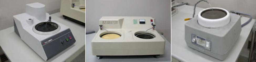
Figure | Mechanical Polishing System
Precision grinding equipment can gradually remove chip material by controlling grinding pressure and grinding speed, commonly used for large area material removal or layer flattening treatment in the early stages of IC delayering. -

Image | Reactive Ion Etching (RIE)
Reactive Ion Etching (RIE) utilizes plasma reactions and ion bombardment mechanisms to precisely remove metal layers or dielectric layer materials from chips, allowing for control over etching rates and directionality, commonly used in IC de-layering and microstructure processing.
-
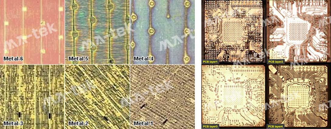
Image | Optical Microscope Imaging (OM Imaging)
Through optical microscopy observation of the metal wiring structure after IC delayering, the wiring configuration and structural distribution of different metal layers (Metal 1 to Metal 6) can be quickly identified. -
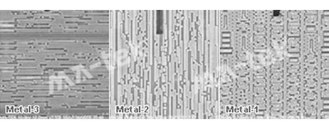
Image | Scanning Electron Microscope Imaging (SEM Imaging)
Using scanning electron microscopy (SEM) to observe the circuit structure after layer removal can obtain higher resolution images of metal wiring and via structures, assisting in the analysis of fine process defects and circuit details.


