
TEM transmission electron microscope
Transmission Electron Microscope (TEM), also known as transmission electron microscope, is a high-resolution microscopic analysis technique that uses a high-energy electron beam to penetrate ultra-thin samples and form images. Since the wavelength of the electron beam is much smaller than that of visible light, the resolution of TEM can reach nanometer or even atomic scale, making it an important tool for observing the internal microstructure, lattice arrangement, and nanoscale defects of materials.
In semiconductor processing, nanomaterials research, and electronic component failure analysis, TEM can directly observe the internal structure of materials, such as crystal arrangement, interface structure, dislocations, and grain boundaries, and can further conduct nanoscale elemental analysis. Through the high-resolution images and material analysis capabilities of TEM, researchers can gain in-depth understanding of material properties and component structures, which play a critical role in advanced process development and product reliability assessment.
Transmission Electron Microscopy (TEM) mainly utilizes a high-energy electron beam to penetrate extremely thin samples (usually less than 100 nm) and forms images through the scattering and diffraction of electrons with the material's atoms. When the electron beam passes through the sample, it generates signals such as transmitted electrons, scattered electrons, and diffracted electrons. After focusing and imaging through an electromagnetic lens system, the fine structure and crystal arrangement of the material can be observed. To enhance the brightness of the electron beam and the imaging resolution, TEM equipment often employs a lanthanum hexaboride (LaB6) electron gun or a Field Emission Gun (FEG). The field emission electron gun has the characteristics of high brightness and low energy spread, allowing the TEM imaging resolution to reach atomic levels, enabling clear observation of nanomaterials and lattice structures.
TEM can be combined with various material analysis techniques. Through these analysis techniques, TEM can not only provide high-resolution images but also conduct nanoscale elemental analysis and crystal structure analysis.
-
Energy-dispersive X-ray spectroscopy (EDS, EDX, EDXS, or XEDS)
-
Electron Energy Loss Spectroscopy (EELS)
-
Selected Area Electron Diffraction (SAED)
Scanning transmission electron microscope (STEM) is a technique that combines electron beam scanning functionality with different detectors for imaging. The detectors used include high-angle annular dark field detector (HAADF), low-angle annular dark field detector (LAADF), bright field detector (BF), and other imaging techniques. STEM combined with HAADF detector can produce images related to atomic number contrast (Z-contrast).
In recent years, equipment suppliers such as Bruker, Thermo Fisher Scientific (formerly FEI), and JEOL have developed large-area EDX detectors and multi-detector configurations, significantly improving element detection efficiency, with element detection sensitivity below 0.1%, greatly enhancing the capability of TEM in nanoscale material analysis.
- Nanostructure and lattice observation: TEM can directly observe the lattice structure of materials at the nanoscale to atomic scale, used for analyzing the crystalline arrangement of materials, dislocations, grain boundaries, and defect structures.
- Thin film and interface structure analysis: High-resolution cross-sectional observation can be performed on multilayer thin film structures to analyze the interface quality of metal layers, dielectric layers, and semiconductor materials.
- Element composition and nanoscale component analysis: Through EDX or EELS analysis, element identification and distribution analysis can be conducted in nanoscale regions to determine material composition and contamination sources.
- Semiconductor process defect analysis: It can observe fine defects in advanced process components, such as lattice defects, interface defects, or nanoscale material changes.
- Material research and nanomaterial analysis: TEM has important application value in the research of nanomaterials, metal alloys, thin film materials, and advanced functional materials.
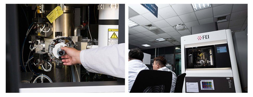
MA-tek has long been deeply involved in the field of semiconductor material analysis and failure analysis, establishing a complete TEM analysis capability. Through high-resolution TEM equipment and a comprehensive analysis platform, MA-tek is able to deeply analyze material microstructures and nanoscale defects, assisting customers in improving product reliability and accelerating advanced process development.
- High-resolution TEM analysis capability:Can provide microstructure observation and lattice analysis from nano to atomic scale.
- Precision sample preparation technology:By combining techniques such as FIB and ion milling, high-quality ultra-thin samples can be prepared.
- Advanced Element Analysis Platform:Combining EDX and EELS technologies, providing nanoscale material composition and chemical analysis.
- Cross-technology integration analysis capability:TEM can be integrated with analysis techniques such as SEM, FIB, X-ray, SAT, and electrical measurements to establish a complete failure analysis process.
-
Atomic Resolution Imaging
-
Selected Area Electron Diffraction (SAED)
-
Micro-area elemental analysis (EDX / EDS)
-
Elemental Mapping at the Nano Scale
-
Chemical bonding and electronic structure analysis (EELS)
In TEM/EDX analysis, the elemental ratios may be influenced by various factors, such as: differences in specimen thickness, element absorption effects, detector geometry, and electron beam scattering range. Therefore, EDX analysis results are usually used for determining elemental composition trends. If a closer theoretical ratio is needed, adjustments can be made through specimen thickness correction or standard sample correction.
1. An element concentration of about 5 wt% or more can be stably detected.
2. With a high-sensitivity detector and optimal analysis conditions, the element analysis capability can be further enhanced.
1. When the sample thickness is about 100 nm, an observation area of approximately 10 × 10 μm can be prepared.
2. If the sample thickness is thicker (about 800–900 nm), an observation range of approximately 25 × 12 μm can be prepared.
The actual preparable range still needs to be adjusted according to the material properties and sample structure.
When the thickness of the film or the grain size of the material to be tested is greater than 200 nm, SAD can be used to analyze the crystal structure. If the grain size is less than 200 nm, Nanobeam Diffraction (NBD) can be used instead. The electron beam size of NBD is approximately 3–5 nm, making it suitable for nanoscale crystal structure analysis.


