
C-AFM conductive atomic force microscope
C-AFM (Conductive Atomic Force Microscopy) conductive atomic force microscopyis based on Atomic Force Microscopy (AFM) and integrates conductive probes and voltage application mechanisms to achieveSimultaneous measurement of surface morphology and local current signalshigh-resolution electrical analysis technology.
AFM was invented in 1985 by Gerd Binnig from IBM Zurich Research Center and Calvin Quate from Stanford University, with the main purpose of allowing non-conductive samples to be scanned using probe microscopy. Unlike scanning tunneling microscopy, AFM detects the van der Waals forces between the probe and the sample atoms, making it applicable to various types of materials including conductors, semiconductors, and insulators. C-AFM further applies a bias voltage at the tip or sample in contact mode, allowing the probe to simultaneously measure the current distribution at each contact point while scanning the surface, thereby accurately locating electrical anomalies at the nanoscale.
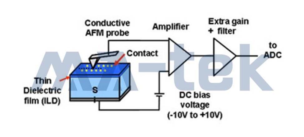
During the AFM scanning process, the interaction between the atomic tip of the probe and the surface atoms of the sample causes slight deflections in the cantilever. The system detects the changes in the cantilever optically to create surface topography.
C-AFM on this basis:
-
Apply DC bias (e.g., -10V to +10V) to the tip or sample.
-
Measure the current signals at each scan point
-
Improve signal sensitivity through amplifiers and filtering systems
-
Simultaneously establish a current distribution map (Current Map)
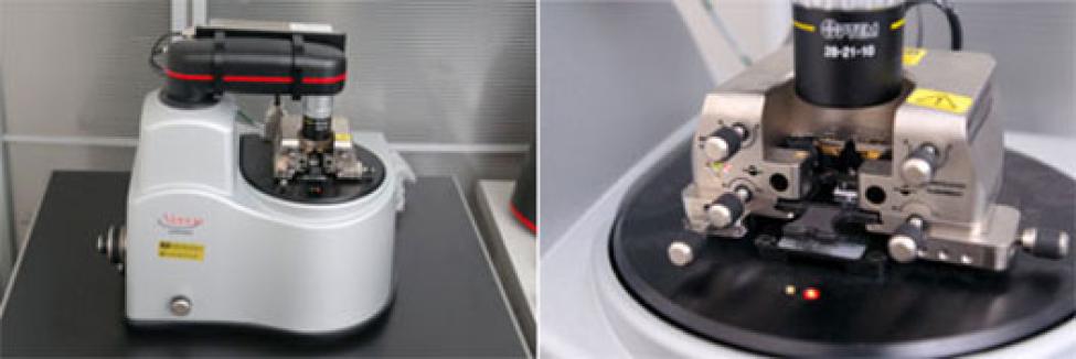
C-AFM is particularly suited for identifying localized electrical issues in semiconductor processes and component failure analysis, including high contact/via resistance, poor contact or localized conduction anomalies, junction leakage, gate oxide leakage, and dielectric layer defects. Through the comparison of Topography and Current Maps, it allows for direct comparison of structural and electrical differences, accurately pinpointing problem areas.
In addition to image analysis, C-AFM can perform voltage-current (I-V) curve measurements at specified points, comparing the electrical behavior of different areas. Through the I-V curve, it can determine:
-
Ohmic contact or Schottky contact characteristics
-
Contact window types (P+ / N+ / Poly contact)
-
leakage conduction mechanism
-
Oxide layer tunneling or breakdown behavior
-
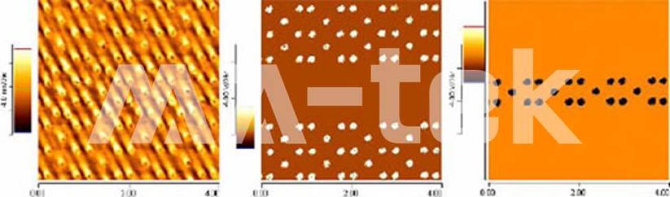 Figure | C-AFM can simultaneously obtain surface morphology images and current intensity signals (a) Topography, (b) Current with +1V bias, (c) Current with -1V bias
 -
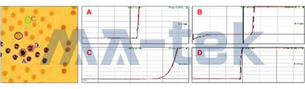 Figure | C-AFM measured voltage-current curves for points (A, B, C, D)


