Defect Localization
With the popularity of advanced packaging (2.5D/3D IC, Fan-Out, SiP) and high-power components, the internal structure of packaging has become increasingly complex, and any minor defects may lead to electrical anomalies or reliability failures. Through non-destructive and high-resolution analysis techniques, potential defect locations within the packaging can be accurately identified without compromising the integrity of the samples.
Common detectable defect types include internal cracks in the package, delamination, voids, solder joint anomalies, poor die attach, and wire bond issues. By cross-validating various imaging and analysis methods, the failure range can be quickly narrowed down, serving as an important basis for subsequent cutting, cross-sectional analysis, and root cause determination.
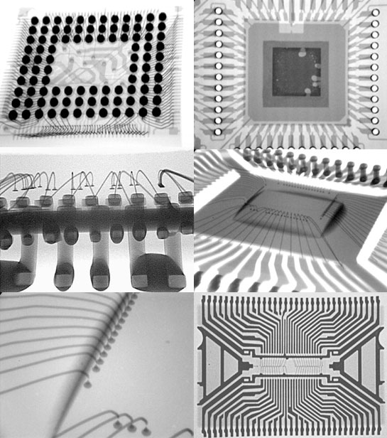
X-ray Photography Examples
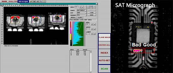
Scanning Acoustic Microscope
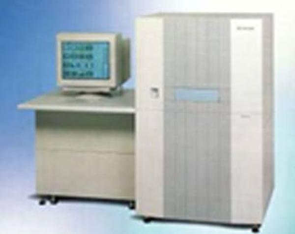
- Package crack
- Delamination
- Die crack
- Void in resin
- Poor die attachment
- poor wire bonding
MA-tek is designed for precision parts and semiconductor packaging, combining industry-leading imaging speed and resolution to provide comprehensive failure analysis solutions:
-
Ultimate imaging performance:equipped with0.5 μm ultra-high resolutionto accurately capture micron-level defects.
-
High detection speed:up to 1000 mm/secThe scanning speed greatly improves the detection efficiency in production lines and laboratories.
-
Omnidirectional scanning mode:Supports A-scan, B-scan, C-scan, S-image, and T-scan to meet the depth analysis needs from points, lines, surfaces to cross-sections.
-
Real-time dynamic 3D:Provides 3D imaging and real-time 3D visualization technologyto make the location and spatial structure of defects clear at a glance.