
EBIC Electron Beam Induced Current Analysis Technology
In advanced semiconductor processes, the component size continues to shrink, and the transistor structure has evolved from traditional planar MOSFET toFinFET and GAA architecturemaking it more difficult to locate issues such as junction defects, gate oxide leakage, and junction leakage.
EBIC (Electron Beam Induced Current) is an important SEM failure analysis technique.It is one of the important electrical localization methods in SEM Failure Analysis. This technique utilizes electron-hole pairs generated by the interaction of the electron beam with semiconductor materials, forming a current loop through an external probe. By analyzing the current image, it is possible to interpret the junction profile, defect locations, and leakage areas, thereby identifying the root cause of component failure.
EBIC analysis is conducted in a scanning electron microscope (SEM) environment. When the electron beam scans a semiconductor sample, the energy of the electron beam generatesElectron–Hole PairsIf the electron beam scanning position is located atnear p-n junctions or depletion regionsThe electrons and holes are influenced by the built-in electric field and are separated, moving in different directions. When the sample forms an electrical circuit through the probe, the current generated by the movement of these carriers is measured and amplified, and then converted into EBIC current images.
By observing the current intensity distribution in EBIC images, engineers can clearly identify: p-n junction locations, junction profiles, leakage areas, and defect locations.
EBIC technology has significant value in semiconductor process development and failure analysis. Since the electron beam can scan the material surface at the nanoscale and generate current signals, it allows engineers to observe electrical anomaly areas without damaging the sample. Therefore, EBIC is often used for analysis:
Gate Oxide Breakdown:When the gate oxide layer breaks down, local current paths appear as bright spots in the EBIC images, allowing engineers to quickly locate defect positions.
Junction Leakage:EBIC can observe junction leakage areas and analyze the impact of junction defects on the electrical properties of the device.
Diffusion Length Measurement:Through the EBIC current signal attenuation characteristics, the carrier diffusion length can be estimated, further assessing material quality and process conditions.
Observation of semiconductor junction profile:EBIC can clearly present the profile of p-n junctions and the location of depletion regions, which is of significant value for process structure research.
In advanced process IC failure analysis, a single analysis technique often struggles to completely locate defects. Different types of defects, such asOpen, Short, Leakage, or High Resistanceneeds to be combined with different electrical localization techniques for cross-validation.
MA-tekThrough integrationEBIC, EBAC, EBIRCH and OBIRCHAdvanced positioning technologies can quickly identify defect locations for different failure modes, and further confirm root causes by combining with physical analysis methods such as FIB and TEM.
As the process nodes move towards5nm, 3nm, and even 2nmThe internal structure of the chip has become more complex, and defect locations are often found in deep metal layers or at the nanoscale junctions.
Through the cross-application of different analysis techniques, it is possible to:
-
Increase the success rate of defect localization
-
Reduce misjudgment
-
shorten analysis time
-
Improve the success rate of subsequent FIB/TEM sample preparation.
Therefore, in advanced process failure analysis,EBIC, EBAC, EBIRCH and OBIRCHhas become an indispensable electrical localization tool.
| Analysis technology | Main Principle | Applicable defect types | Application |
|---|---|---|---|
| EBIC | The electron beam generates electron-hole pairs and forms current images. | Junction leakage、Gate oxide breakdown | Interface defect localization, oxide layer breakdown analysis |
| EBAC | Electron beam excites the current in metal wires and tracks the conduction path. | Metal open, High resistance | Multi-layer metal interconnect open circuit localization |
| EBIRCH | The electron beam causes localized temperature rise leading to resistance change. | Metal short、High impedance | Metal short circuit and high impedance defects |
| OBIRCH | Laser localized heating causes resistance changes | Short defect、Leakage path | Packaging and chip short circuit localization |
MA-tekLong-term focus on semiconductor material analysis and failure analysis, establishing a complete advanced process analysis platform. In the application of EBIC technology, MA-tek can combine multiple electrical and material analysis techniques to provide a more comprehensive defect localization and root cause analysis capability, through integration:
-
SEM-based Nano-probing
-
EBAC / EBIRCH Electron Beam Induced Analysis
-
OBIRCH laser resistance variation localization
-
C-AFM conductive atomic force microscope
-
FIB precise cross-section sample preparation
-
TEM nanostructure analysis
This can form, from Electrical defect localization → Physical cross-section analysis → Material root cause verificationThe complete failure analysis process. In the analysis of advanced processes and high-reliability products, this integration capability can effectively shorten the localization time and improve the success rate of subsequent analyses, providing customers with efficient and highly reliable failure analysis solutions.
-
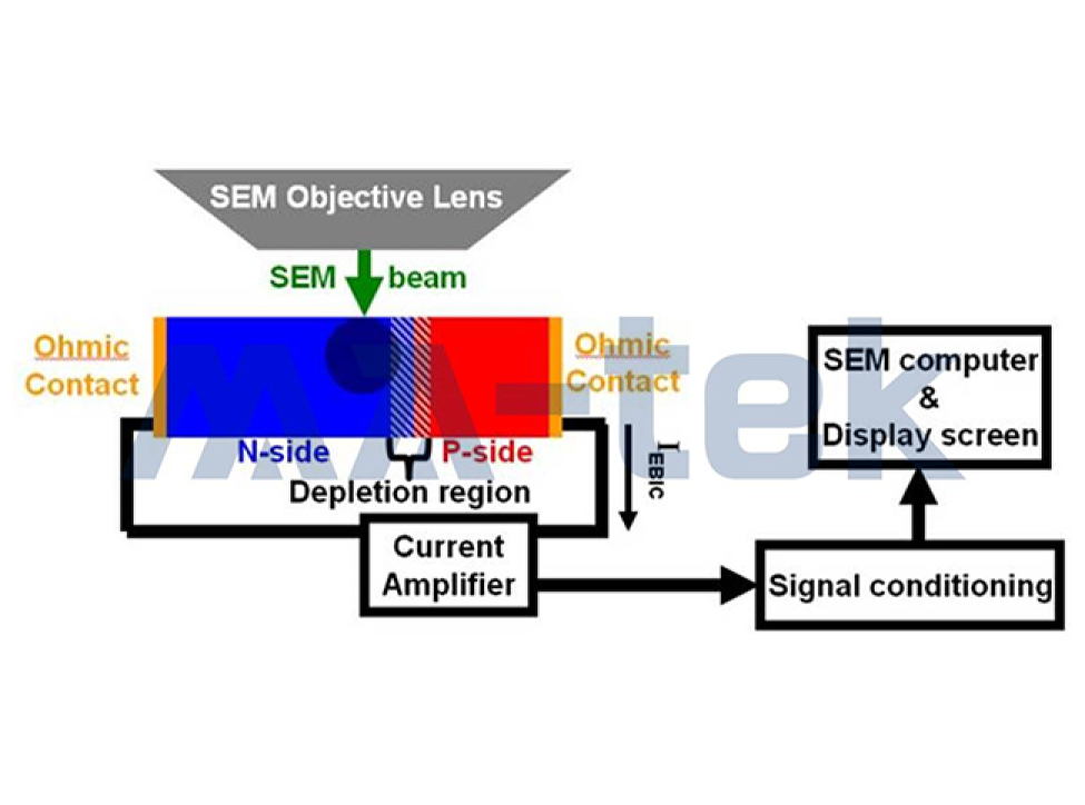
Diagram | Principle diagram of EBIC (Electron Beam Induced Current)
The working principle of EBIC is based on the generation ofelectron–hole pairsUnder the action of the built-in electric field in the depletion region of the p-n junction, electrons and holes are separated, forming a current signal. Through the electrical circuit formed by external probes, the current is converted into an EBIC image via a current amplifier and signal processing system, allowing engineers to observe the junction position and locate electrical defects.
-
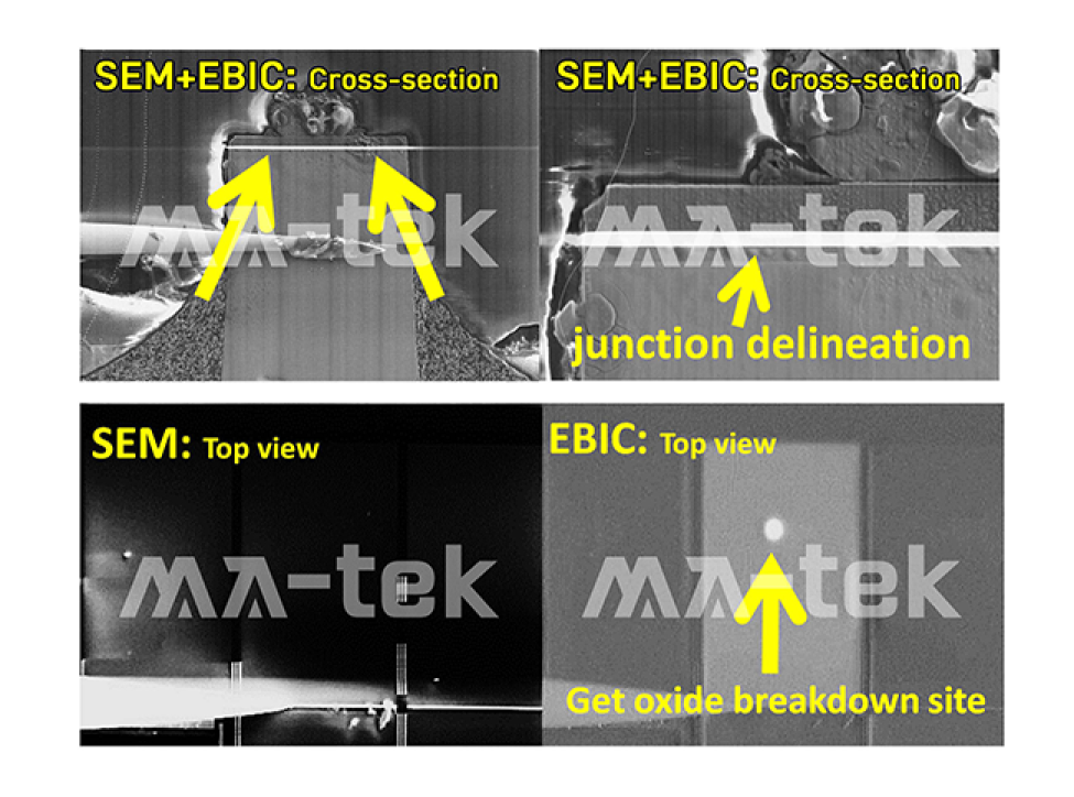
The image shows that EBIC technology can locate junction defects and the breakdown position of the gate oxide layer.
EBIC (Electron Beam Induced Current) combines SEM images and current signals, allowing observation at a microscopic scale.p-n junction delineationand the region of electrical anomalies. When the electron beam scans to the defect location, a stronger EBIC current signal is generated due to the local electric field and carrier separation effect, causing the defect area to appear as bright spots in the EBIC image. By comparing the SEM image with the EBIC current image, precise positioning can be achieved.Gate oxide breakdown, junction leakage and other electrical defect locationsIt is one of the important technologies for advanced process failure analysis.


