
2D X-ray
In the semiconductor packaging and electronic assembly process, many critical structures are located inside the components, such as solder joints, wire bonds, silver paste, and lead frames. If these internal structures have voids, poor contact, or structural abnormalities, they will directly affect the reliability of the components and the yield of the products.
2D X-ray (Two-dimensional X-ray Inspection)In a non-destructive manner, the X-rays generated by high-energy impacts on metal targets have penetrating characteristics, which can be used to observe and determine whether there are phenomena such as voids, HIP, or Hop inside advanced packaging. This tool can also quickly confirm defects such as broken wires and severe melting inside the package.
The basic principle of X-ray detection is to use X-ray radiation to penetrate the object being inspected. When X-rays pass through different materials, their absorption capacity varies due to differences in material density and atomic number. The X-rays that pass through the sample are received by an imaging detector and converted into a visible image, in which:
-
Higher density metal materials (such as copper, gold, tin) will present a deeper contrast.
-
Lower density materials (such as packaging resin) will appear as lighter images.
Through this density difference, the internal structure of IC packaging can be clearly observed, such as wire paths, solder point morphology, or internal voids and other defects.
-
PCB assembly defect detection
2D X-ray equipment is particularly suitable for PCB assembly inspection, allowing for quick assessment of solder quality and component bonding conditions, such as:
-
Soldering status of active components and passive components
-
Void ratio analysis of solder joints
-
BGA / QFN solder ball structure inspection
-
PCB assembly defect detection
-
-
Internal structure inspection of electronic components
2D X-ray can also be used to observe the internal structures of various electronic components, such as:
-
Sensor
-
Relay
-
Fuse and fusible link
-
Coil / Winding
-
IC packaging and die attach
-
Wire Bond structure
-
MA-tekLong-term focus on semiconductor material analysis and failure analysis, establishing a complete packaging and structural inspection platform. In X-ray inspection, MA-tek can combine various analytical techniques to provide more comprehensive defect localization capabilities, forming fromInternal structure inspection → Defect localization → Microscopic analysis → Root cause determinationThe complete analysis process helps customers quickly grasp product quality and improve reliability.
MA-tek has introduced multiple high-resolution X-ray inspection systems, which can provide non-destructive testing services for different packages and electronic components. Through the high-resolution X-ray imaging system, it is possible to accurately observe the status of packaging and soldering structures.
-
Feinfocus FXS-160.40 TIGER X-RAY
-
Dage XD7600NT X-ray Inspection System
-
 Image | Feinfocus FXS-160.40 TIGER X-ray System
 -
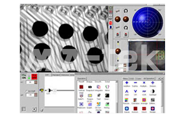 Image | X-ray inspection operation and image control interface
 -
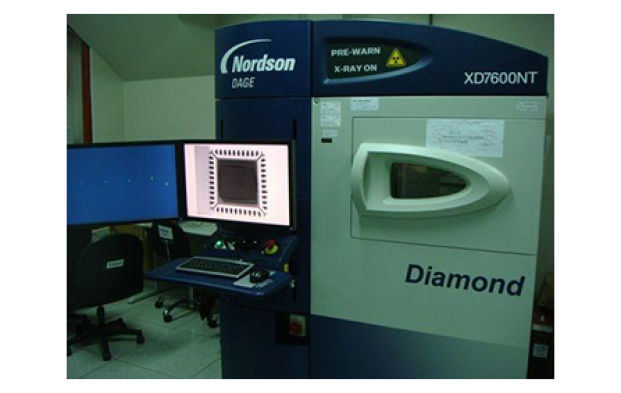 Image | Dage XD7600NT X-ray Inspection System
-
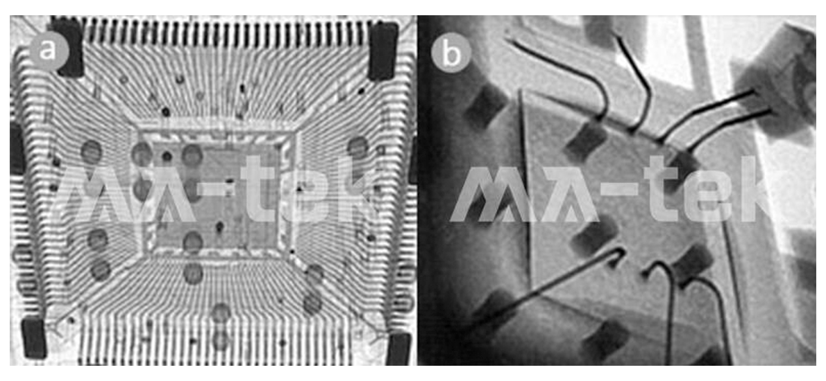
Image | X-ray image of internal structure of IC packaging
Observe the internal wire bonding and die structure of the package, and check for any contact failures or structural abnormalities.
-
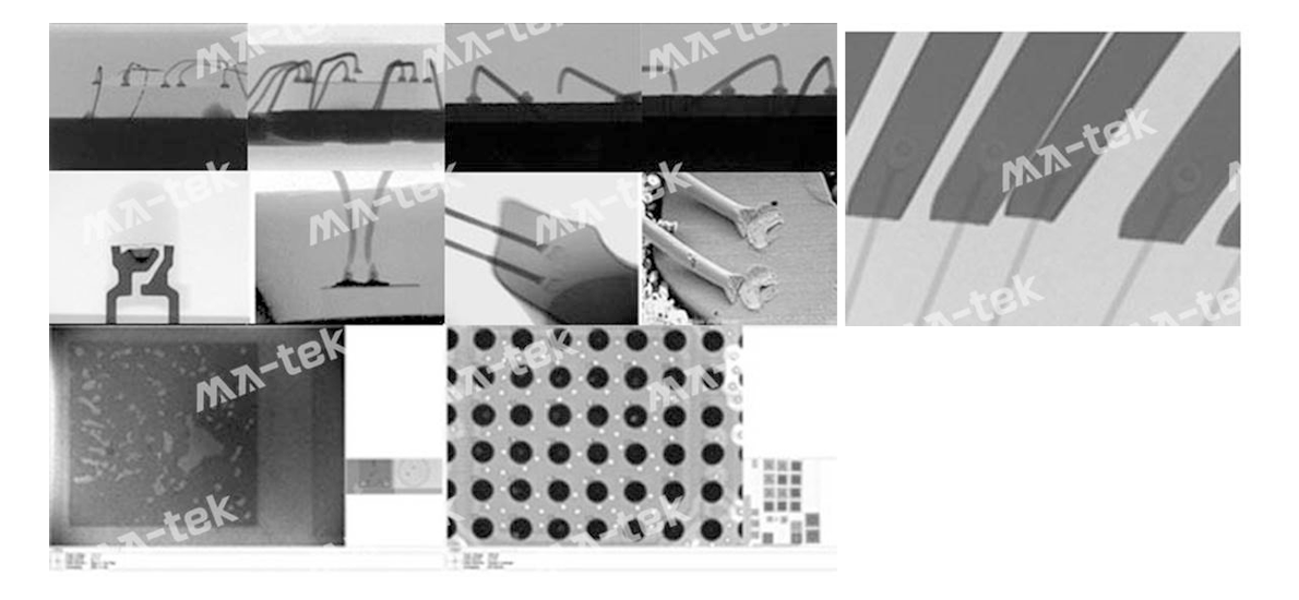
Image | Internal defects of electronic components X-ray image
Display issues such as solder voids, soldering anomalies, or material defects, assisting engineers in quickly locating structural anomalies.
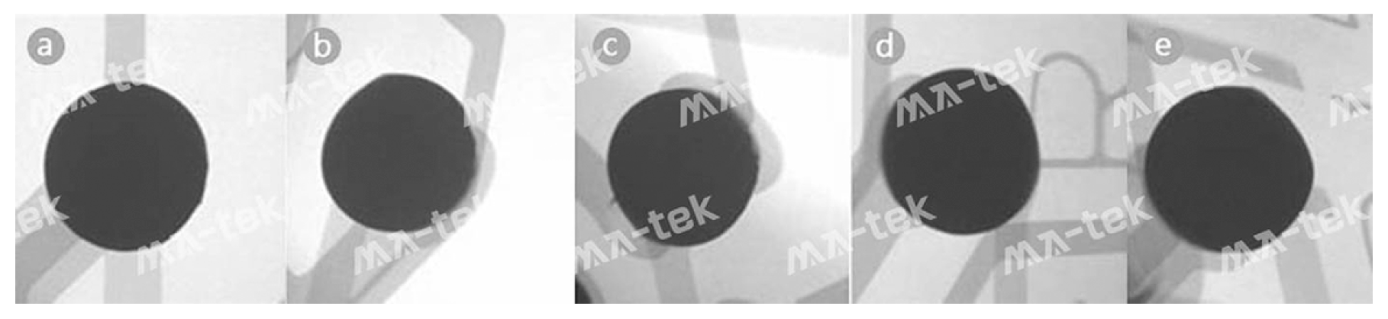
Image | Multi-angle inclined X-ray inspection
(a) 0° Tilt, 0° Rotate (b) 55° Tilt, 45° Rotate (c) 55° Tilt, 135° Rotate (d) 55° Tilt, 225° Rotate (e) 55° Tilt, 315° Rotate
By observing at different tilt and rotation angles, the structure of solder joints and internal defects can be more clearly identified.
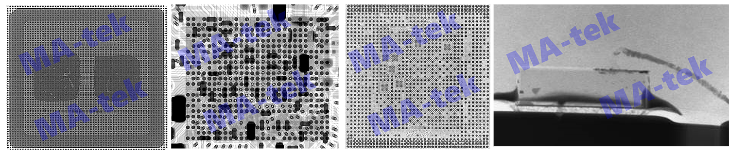
Figure | 2D X-ray inspection results
(a) Advanced packaging bottom solder ball distribution images can observe the occurrence of voids and abnormal solder joint conditions in local areas.
(b) X-ray images of the internal wiring and component structure of the package show abnormal density in local metal areas, suspected to be due to HIP/HOP or uneven material accumulation.
(c) The image of the chip area solder joint arrangement shows inconsistent contrast in some solder balls, indicating possible soldering defects or internal void defects.
(d) Side view cross-sectional image of the package shows deformation and localized collapse of the internal metal layer, suspected structural anomalies caused by broken wires or localized melting.


