
Nano Probe Electrical Measurement Technology
As the advanced IC manufacturing process continues to shrink to the nanometer node, the density of transistors has significantly increased. Accurately locating the electrical failure position at such a small scale has become a core challenge in advanced failure analysis and process verification.Nano-ProbingIt is based on high spatial resolution atomic force microscopy (AFM), combined with a multi-probe nano-electrical detection system, for non-destructive analysis technology that directly measures electrical properties and locates failures of a single transistor at the nanoscale, through:
-
Tapping Mode: Obtaining high-resolution surface morphology
-
Contact Mode: Conducting precise electrical measurements
Avoiding charge accumulation and measurement offset issues that may be caused by electron beams is an important tool for advanced logic processes and high-end memory analysis.
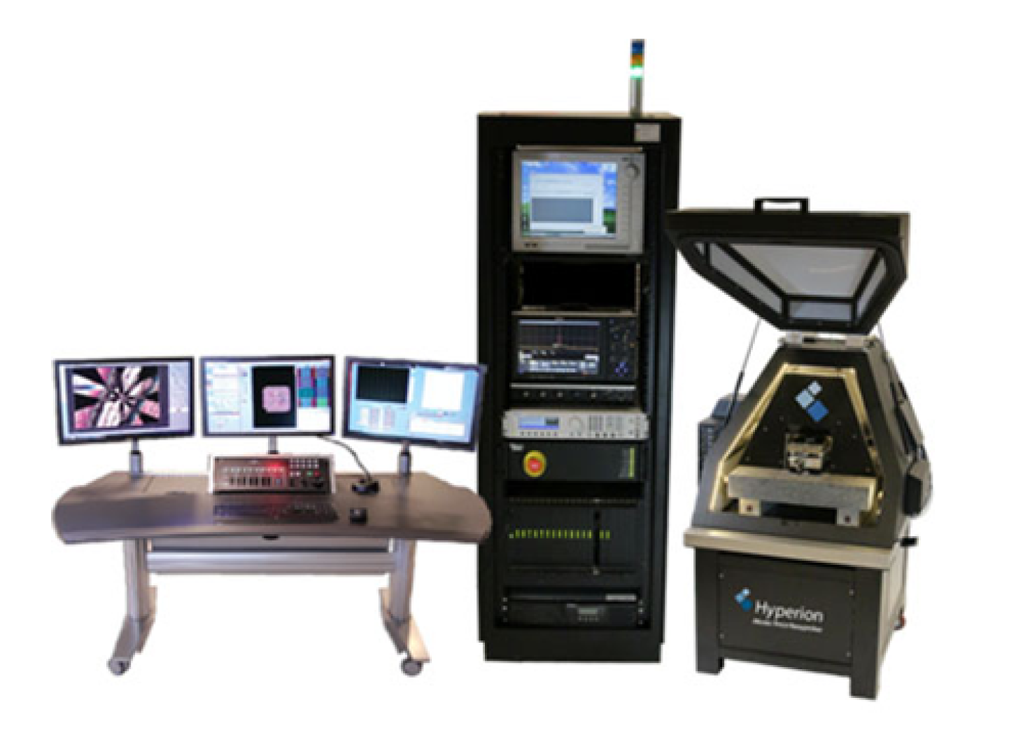
AFM-based Nano-probing technology integrates high-resolution imaging, pico-current analysis, and SCM doping interpretation to accurately identify failure locations in individual transistors at the nanoscale, providing reliable electrical diagnostics for advanced processes and high-density ICs.
MA-tekWith complete nano-electrical analysis integration capabilities, AFM-based Nano-probing can be combined withC-AFM,OBIRCH,PEM-CCD / InGaAs,Thermal EMMII-V / C-V electrical measurements,FIB and TEM sample analysis,Form a one-stop failure location and physical analysis process.
Through cross-technology validation and professional interpretation experience, the positioning time can be significantly shortened and the success rate of root cause determination can be improved.
-
Non-destructive nano-electrical measurement solution
AFM-based Nano-probing has the following key advantages:
-
High spatial resolution (approximately 10 nm laterally)
-
No electron beam interference
-
Tapping / Contact Dual-mode Integration
-
Pico-current high sensitivity analysis
-
SCM two-dimensional doping interpretation capability
-
Applicable to single transistor measurement
In advanced processes, this non-destructive measurement method without electron beam interference has high value for subsequent FIB, TEM, or physical failure analysis.
-
-
Nano electrical analysis applicable to 10 nanometer process nodes
AFM-based Nano-probing technology capabilities include:
-
Support for 10 nanometer process nodes
-
Eight sets of nano-probes
-
Tungsten probe curvature radius 15–35 nm
-
Low contact resistance < 30 Ω
-
Ultra-low positional drift rate of about 1 nm
-
Precise positioning within a range of 200 micrometers
-
Nitrogen (N₂) chamber device prevents sample oxidation
-
Through Tapping Mode AFMScan the sample surface to create a clear nanoscale topography map, accurately pinpointing the target component's location. In Contact Mode, a tungsten nano-probe contacts the target transistor to perform single-point electrical measurements. Since the measurement process does not require an electron beam, it can avoid charge accumulation effects, electrical characteristic drift, and component misjudgment, combined with high sensitivity.pico-current (pA level) imaging systemIt can clearly present weak leakage current or local conduction anomalies.
In AFM-based Nano-probing electrical measurement processIn this context, Tapping Mode and Contact Mode play different yet complementary roles, serving as core technologies to ensure measurement accuracy and sample integrity.
Tapping Mode (Tapping Mode AFM) - High-resolution nano surface morphology construction
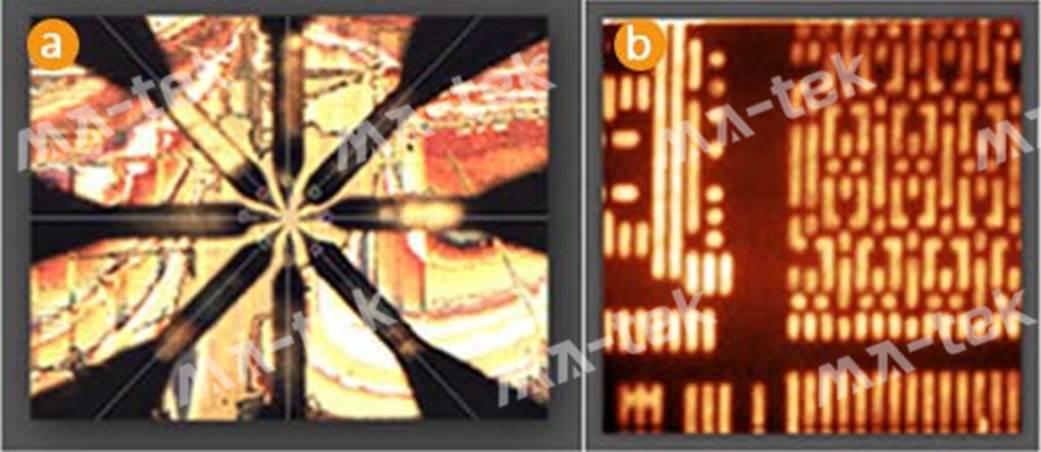
(a) Eight sets of probe OM images (Multi-probe layout)
(b) Tapping Mode AFM high-resolution morphology map, used to establish ROI and precise positioning coordinates for target components.
-
Reduce friction damage between the probe and the sample.
-
Suitable for miniaturization processes and fragile structures
-
Provide accurate ROI (Region of Interest) positioning reference.
-
Achievable lateral resolution of approximately 10 nm.
After completing the morphology positioning, the system switches toContact ModeThe conductive probe forms stable contact with the target component and applies a bias voltage for electrical measurements. It can perform single-point current measurements, I-V curve scanning, local conduction characteristic analysis, and resistance anomaly diagnosis. Since the measurement process does not use an electron beam (e-beam), it can avoid charge accumulation and electrical offset issues, ensuring that the measurement results are closer to the original characteristics of the component. The system is equipped with a force feedback control mechanism, allowing for precise adjustment of the probe's contact force, achieving the best balance between stable conduction and structural protection.
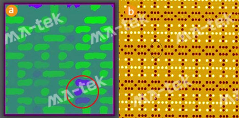
(a) Pico-current imaging: presents local leakage/conduction anomaly locations and current paths with pA level sensitivity.
(b) SCM image: Establish the doping distribution of the N/P region to assist in interpreting the failure mechanism caused by doping anomalies.
AFM-based Nano-probing Integration:
-
Pico-current Imaging (pA level current detection, sensitivity up to 5 pA)
-
Scanning Capacitance Microscopy(SCM)
Pico-current imaging can visualize extremely small leakage currents or local conduction anomalies, clearly presenting the current paths.SCM can establish two-dimensional doping images, distinguishing between N-type and P-type regions, providing key interpretive basis for electrical failures caused by abnormal doping distribution.
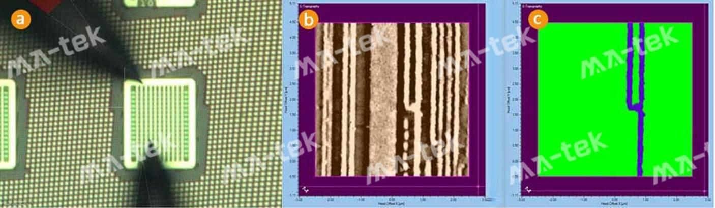
Figure | Multimodal cross-validation of ROI area (OM → AFM → Pico-current)
(a) ROI optical image: quickly identify target area
(b) ROI AFM morphology: Establishing nanoscale structures and coordinate alignment
(c) ROI Pico-current: Directly displays abnormal current distribution, locking onto a single component/local defect location.
AFM-based Nano-probing can accurately target components within a range of 200 micrometers and perform on specific ROIs:
-
Morphology comparison
-
Local conductivity measurement
-
Current path reconstruction


