
Board-level drop test
Board Level Drop Test is mainly used to evaluateAssembled circuit board (PCBA)the reliability performance under instantaneous mechanical impact, with a particular focus onStructural integrity of solder joints between surface mount components and the circuit board。
When electronic products accidentally fall during manufacturing, assembly, transportation, or daily use, the circuit board will bend and deform due to instantaneous acceleration, causing the solder joints to endure significant tensile and shear stress. The Board Level Drop Test simulates such real-life scenarios through standardized accelerated impact conditions to assess whether the solder joints will develop cracks, fatigue damage, or instantaneous breakage, ensuring that the product has sufficient mechanical durability throughout its lifespan.
The core purpose of the board-level drop test is to:
-
Evaluate the reliability of PCBA in portable electronic products under drop impact.
-
Comparing the drop impact resistance of different solder materials, packaging forms, component layouts, or PCB designs.
-
Verify the durability and lifespan of solder joints under repeated accelerated impact.
-
Provide important basis for product design and material selection.
Due to the circuit board generated during the fallBoard Bendingis often the main cause of solder joint failure, so this test is widely used for reliability verification of mobile phones, wearable devices, consumer electronics, and automotive modules.
The board-level drop test followsJEDEC JESD22-B111International standards implementation ensures that test results are consistent and comparable.
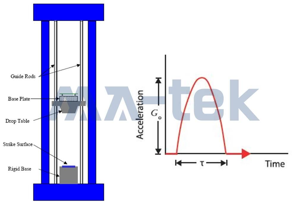
Testing Process and Methods
During the test, the four corners of the PCBA to be tested are secured with screws to the base plate of the drop test machine, placing the circuit board in a controlled and repeatable fixed state. After raising the drop table to the specified height, it is allowed to fall freely, impacting the strike surface on the machine, generating a high acceleration impact momentarily. During each drop impact process, the system synchronously measures and records the following key parameters:
-
Peak Acceleration
-
Velocity Change
-
Pulse Duration Time
Common standard test conditions are1500 g / 0.5 msThis condition can effectively simulate the instantaneous mechanical stress when the actual product falls.
Failure Assessment | Objective Standards of Real-Time Resistance Monitoring
The board-level drop test is usually paired withreal-time resistance monitoring system (Multi Event Detector System, MEDS)to dynamically detect whether electrical interruptions occur at solder joints during the impact moment, with failure assessment criteria being: when the monitoring system detectsThe resistance value is greater than 1000 Ω in a single impact event., and in the subsequent In five consecutive impacts, at least three instances show resistance values exceeding 1000 Ω, and the duration is 1 millisecond (ms) or longer.This standard can effectively eliminate the impact of instantaneous noise, ensuring that the determination results truly reflect the electrical anomalies caused by the structural damage of the solder joints.
Board-level drop testing has high practical value in the electronics industry and is commonly applied to:
-
Reliability comparison of new solder, new packaging, and new materials
-
Impact resistance analysis of different PCB thicknesses, layer counts, and structural designs
-
Evaluation of solder joint strength for BGA, CSP, QFN, and other packages.
-
Process condition adjustment and solder joint design optimization
Through standardized drop conditions and quantitative failure determination, the risk of early failure of products in the market due to drop impact can be effectively reduced.


