
Chat with us, powered by LiveChat

SEM-based Nano-probing

Under the rapid development of high-performance computing and AI chips, the semiconductor process has officially entered the post-Moore era. The process node has advanced from 7nm to 5nm, and is progressing towards 3nm and 2nm; the component structure has also evolved from planar MOSFET toFinFET and GAAand other three-dimensional structures.


At this nanoscale, traditional AFM-based nano-probing has become difficult to meet the demands for high-resolution positioning and stable electrical measurements.SEM-based Nano-probing (Scanning Electron Microscope Nano-probing Technology)Become the core tool for advanced process single device measurement and failure analysis.


SEM-based Nano-probing can be conducted in a SEM vacuum environment, usingLow acceleration voltage electron beamSuccessfully applied in conjunction with nano-probing.5nm FinFET process node

  • High-resolution morphology observation

  • Single Transistor I-V / C-V Measurement

  • Leakage and short circuit localization

  • RC delay analysis

  • EBIC / EBAC / EBIRCH failure interpretation

SEM-based Nano-probing technology principle

SEM-based Nano-probing is to combineScanning Electron Microscope (SEM)Integrating with a nano-scale mechanical probing system in the same vacuum environment allows engineers to perform electrical measurements and defect localization of individual transistors synchronously under high-resolution imaging conditions.
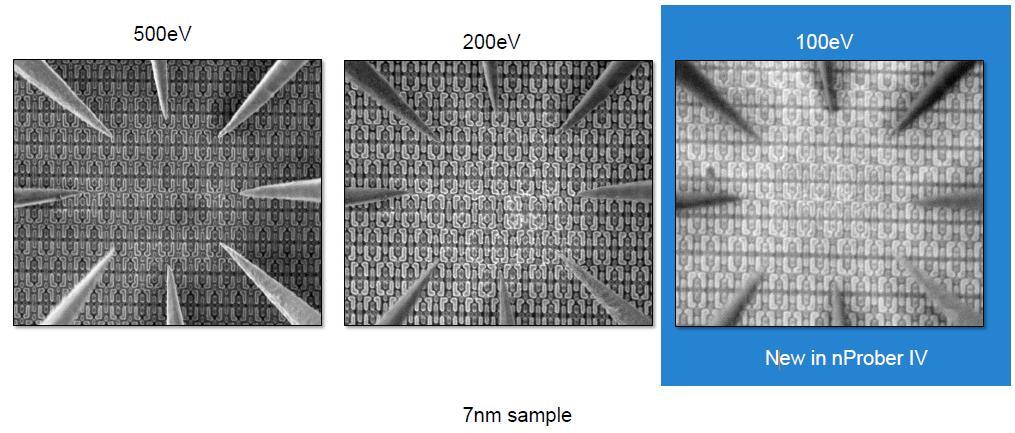
 

Low voltage I-V measurements - Stable electrical characteristics under low kV environment
Figure | Comparison of electrical differences of 7nm devices under different acceleration voltages
When performing electrical measurements in a SEM environment, the electron beam itself may cause charge accumulation on the sample surface and drift in channel characteristics, thereby affecting measurement interpretation. nProber IV supports a minimum operating acceleration voltage of 100eV, which can effectively reduce the interference of the electron beam on the device, making the I-V curve closer to the original characteristics of the device.


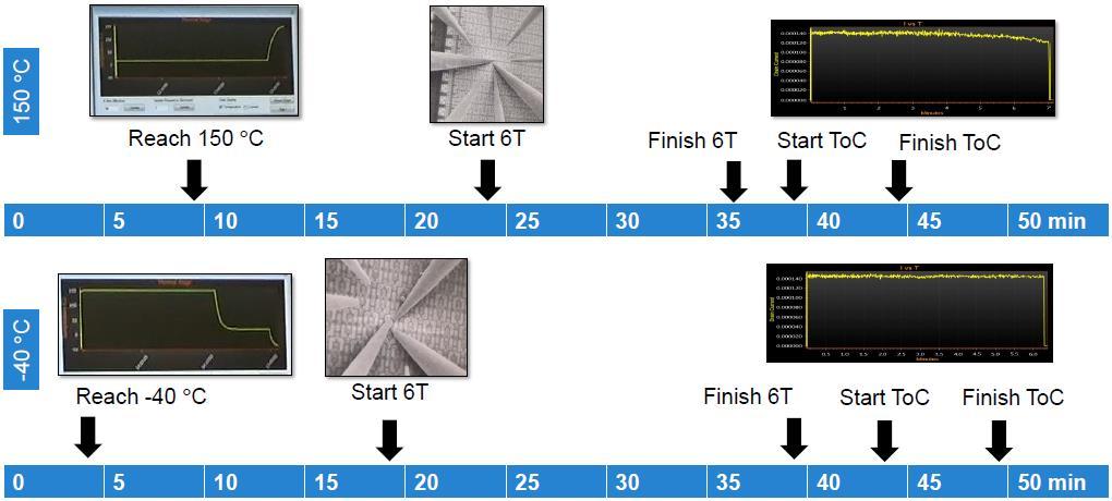
Temperature-controlled stage and environmental electrical analysis -40°C to 150°C dynamic condition verification
Diagram | Component Temperature Variation Electrical Measurement Process Schematic
The reliability verification of advanced chips is not limited to room temperature operation; temperature has a significant impact on leakage, contact resistance, and channel behavior. SEM-based Nano-probing integrates a temperature-controlled stage, allowing electrical measurements to be conducted under environmental conditions ranging from -40°C to 150°C, assisting engineers in evaluating the stability of components under high temperature, high power, and low temperature extreme conditions.


Electron beam-induced failure analysis techniques - EBIC, EBAC, and EBIRCH integrated interpretation.

On the SEM platform, in addition to basic electrical measurements, electron beam induced analysis can also be performed. When the electron beam strikes the sample, electron-hole pairs are generated, which can form measurable current signals, thereby locating defects such as gate oxide breakdown, junction leakage, or metal open and short circuits. By cross-referencing EBIC, EBAC, and EBIRCH techniques, different types of failures can be distinguished, enhancing the accuracy of interpretation.
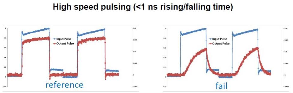


High-speed 750ps Pulsed I-V - Nano-device transient and RC delay analysis
Figure | High-speed Pulsed I-V Transient Waveform Comparison (Reference vs Fail)
At the nanoscale, the effects of resistance and capacitance significantly impact the switching behavior of transistors. nProber IV features 750ps high-speed pulsed I-V capabilities, allowing it to capture the transient waveforms of transistors at the moment of switching, analyze the rise and fall delay times, and compare the differences between normal and failed products, which is crucial for diagnosing RC delay, gate oxide leakage, and contact anomalies.


C-V measurement and channel quality verification
Figure | High-speed Pulsed I-V Transient Waveform Comparison (Reference vs Fail)
At the nanoscale, the effects of resistance and capacitance significantly influence the switching behavior of transistors. nProber IV features 750ps high-speed pulsed I-V capabilities, allowing it to capture the transient waveforms of transistors at the moment of switching, analyze rise and fall delay times, and compare the differences between normal and failed products, which is of critical value for diagnosing RC delay, gate oxide leakage, and contact anomalies.


MA-tek advantages

In advanced processes below 5nm, a single technology can no longer fully determine the root cause of failure.MA-tekWith "cross-technology integration" as the core advantage, SEM-based Nano-probing is incorporated into the complete failure analysis process, rather than being a point measurement.
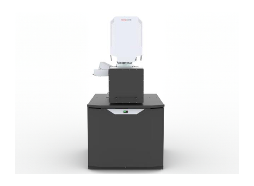
 

Image | nProber IV Fourth Generation SEM-based NanoProber System

MA-tekIntegrating SEM-based Nano-probing into the complete failure analysis process, rather than as a standalone measurement technique. Once the nano probe locates a suspicious area, it can seamlessly connect with AFM-based Nano-probing, C-AFM, OBIRCH, Thermal EMMI, FIB precise sample preparation, and TEM structural verification, forming an integrated platform for Electrical FA and Physical FA.


At nodes of 5nm and below, a single technology has become insufficient to solve complex failure issues. Through cross-technology validation and professional interpretation experience, MA-tek can effectively shorten positioning time, improve the success rate of root cause determination, and reduce rework and misjudgment risks.


The nProber IV fourth-generation SEM-based NanoProber system integrates high-resolution SEM and nano-probing measurement platforms, allowing for single transistor electrical measurements and precise failure localization in a vacuum environment, making it a core device for advanced process nano-electrical analysis.


 

Contact
Contact Window
Shanghai Laboratory

Nanoprobe team

Taiwan Laboratory

Nano Probe team

Privacy Preference Center

We use cookies to allow our website to function properly, personalize content and advertisements, provide social media features, and analyze traffic. We also share information about your usage of our website with social media, advertising, and analytics partners.

View Privacy Policy

Manage Consent Settings

Necessary Cookies

Always Enabled

The operation of the website relies on these cookies, and you cannot disable them in the system. These cookies are usually set based on the actions you take (i.e., service requests), such as setting privacy preferences, logging in, or filling out forms. You can configure your browser to block or prompt you about these cookies, but this may result in certain website functionalities not working.
