
DB P-FIB Dual Beam Focused Ion Beam
Dual Beam Plasma FIB (DP-FIB)It is a high-performance material processing and analysis equipment that combines plasma ion beams with scanning electron microscopy (SEM). Unlike traditional FIB systems that use gallium ions (Ga⁺), P-FIB employs a xenon ion (Xe⁺) plasma ion source, which can provide higher ion beam currents and faster material removal rates.
Due to the higher etching efficiency of the xenon ion beam, the material removal rate of P-FIB can reach that of traditional Ga⁺ FIB.about 20 timesTherefore, it is particularly suitable for cross-section preparation and rapid defect analysis of large-sized structures. This technology has significant application value in advanced packaging, chip backside analysis, TSV structure, and solder joint structure research.
In the dual-beam system architecture, P-FIB is equipped with both electron beam and ion beam optical systems, allowing engineers to observe changes in the cross-sectional structure in real-time using SEM while cutting materials, quickly determining defect locations and structural anomalies.
P-FIB adoptsXe Plasma Ion SourceGenerate high-current ion beams, which are then focused on the sample surface through electromagnetic lenses. When the ion beam bombards the material, it produces a strong material sputtering effect, allowing for the rapid removal of surface material. Compared to Ga⁺ FIB, P-FIB has the following important technical features:
-
Using Xe⁺ ion beams, it can provide higher beam current.
-
The material removal rate has significantly increased.
-
suitable for large-area cross-section preparation
-
Reduce Ga ion contamination issues
In terms of system architecture, P-FIB adoptsDual Beam designTherefore, during the cross-section preparation process, structural changes can be observed simultaneously to ensure the accuracy of the analysis location.
-
Ion Beam System
-
Used for material cutting and cross-section preparation
-
Large-scale rapid etching
-
-
Electron Beam System (SEM)
-
Used for imaging observation and positioning
-
Real-time monitoring of the cutting process
-
Since P-FIB has high-speed material removal capabilities, it has significant advantages in large-scale packaging structures and chip cross-section analysis, when throughThermal Emission Microscopy, Optical Microscope (OM), 3D X-ray or Scanning Acoustic Microscopy (SAT)After non-destructive analysis techniques locate suspected abnormal areas, P-FIB can be further utilized for cross-section confirmation and microstructure analysis.
-
2.5D / 3D IC packaging
-
TSV (Through-Silicon Via)
-
C4 bump / Interposer / U-bump
-
Bond pad / First solder point / Second solder point
-
Solder bump / BGA ball
-
Chip backside analysis
-
MEMS components
-
Packaging and PCB structure
MA-tek has established a completePlasma FIB analysis platformsupports a wide range of cross-section analysis needs for advanced packaging and semiconductor components. Through P-FIB andIntegration of technologies such as SEM, TEM, X-ray, SAT, EMMI, OBIRCH, etc.It can establish a complete failure analysis process from non-destructive analysis to microstructure analysis. Compared to traditional FIB, P-FIB has higher material removal efficiency and greater cross-section processing capability, making it play a key role in advanced packaging and 3D IC analysis.
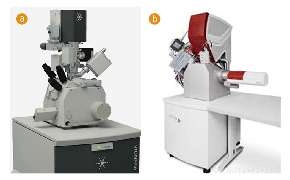
MA-tek introduces high performanceP-FIB analysis system, respectively from FEI (Thermo Fisher Scientific) and TESCANIt can support rapid cross-sectional analysis of large samples and high-resolution image observation.
-
Beam current:1.5 pA – 1.3 µA
-
Landing voltage:2 – 30 kV
-
Ion beam resolution:< 25 nm @ 30 kV
-
Automated large-area processing capability
-
Maximum cutting size can reach500 µm × 500 µm
-
High efficiency material removal and cross-section preparation
-
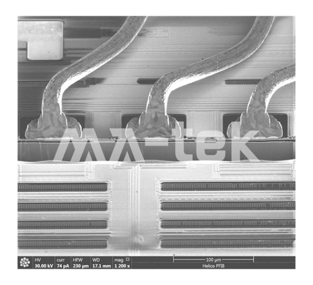 Figure | Observation of Bond Pad and Wire Bonding
P-FIB can quickly create package cross-sections to observe bond pads, gold wire bonds, and metal layer structures, analyzing solder quality and material interface conditions.
-
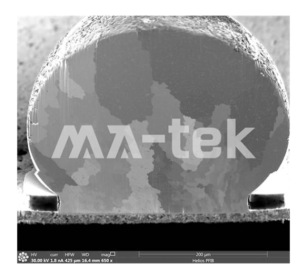 Figure | Observation of solder bump grain structureusing Ion Channeling ContrastThe internal grain distribution and crystallographic structure of the solder balls can be observed.
 -
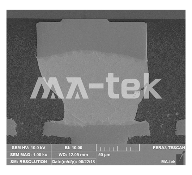 Image | C4 bump cross-section observationUsed for analyzing flip-chip solder joint structures, IMC layers, and bonding quality.
-
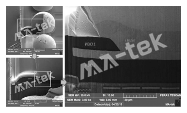 Figure | BGA ball package cross-sectionP-FIB can quickly cut large solder ball structures to analyze solder interfaces and void defects.
 -
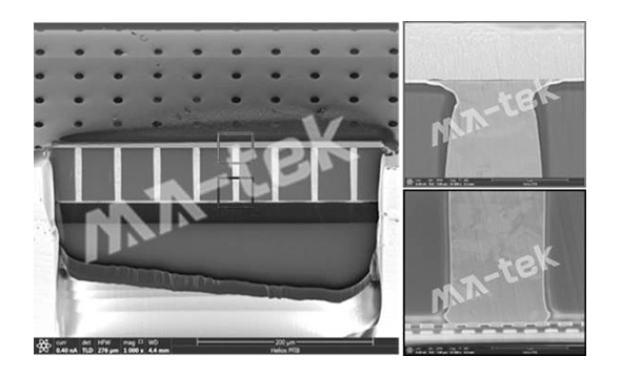 Figure | TSV Structure Analysissuitable for3D IC and advanced packaging TSV structure cross-sectional observation.
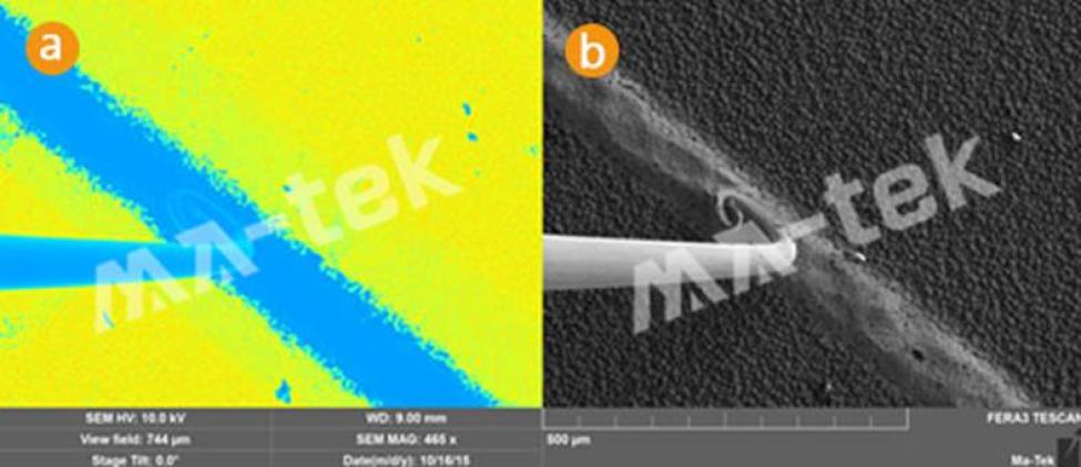
EBIC (Electron Beam Induced Current)
EBIC technology measures the current signal generated by the electron beam bombarding the sample through a probe, forming an EBIC image. By analyzing the distribution of the current signal, the defect locations in semiconductor devices can be determined, such as leakage paths or material defects.
- Cathodoluminescence (CL) images are used to observe the luminescence distribution of materials under electron beam excitation, and can be used to identify differences in material composition or defect locations.
- Secondary Electron (SE) images show the surface morphology and contamination distribution of the sample.
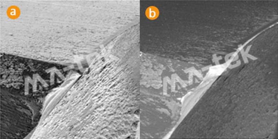
Backscattered Electron Detector (BSE Detector)
The Backscattered Electron Detector (BSE Detector) uses backscattered electron signals to form images. Due to different materials having different atomic numbers, there will be significant material contrast in BSE images, which can effectively identify material composition and interface locations.
- Secondary electron imaging (SEI):The morphology details of the sample cross-section surface are displayed, allowing for clear observation of the surface roughness and microstructural features after material processing.
- Backscattered Electron (BSE) Imaging:Using backscattered electron signals to form material contrast images can distinguish different materials or phase distributions, and clearly present interface structures and material composition differences.
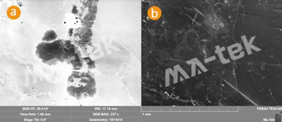
Cathodoluminescence (CL)
Cathodoluminescence (CL) or cathodoluminescence, cathode ray luminescence detectors can analyze the luminescence signals generated by materials under electron beam excitation. Through CL images, the composition of materials, defect distribution, and differences in crystal structure can be determined.
- Cathodoluminescence (CL) imagingDisplays the cathodoluminescence distribution generated by the material under electron beam excitation, which can be used to identify differences in material composition, the location of crystal defects, or contamination particles.
- Secondary Electron (SE) imageThe surface morphology and microstructural features of the sample are presented, allowing for the observation of defects such as surface cracks, contamination, or structural discontinuities.
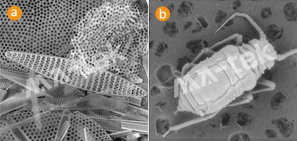
LVSTD low vacuum mode
LVSTD (Low Vacuum Secondary TESCAN Detector) can be used inLow vacuum environment of 1–500 PaThe following operations can reduce the charging effect of the sample and allow for the observation of non-conductive materials and biological samples. Biological samples, moisture-containing materials, and non-conductive materials can be observed through low vacuum mode.
- The SEM image of diatom microstructure in low vacuum mode allows observation of its nanoscale porous shell structure.
- SEM images of micro insect samples in low vacuum mode show surface details and three-dimensional morphology.
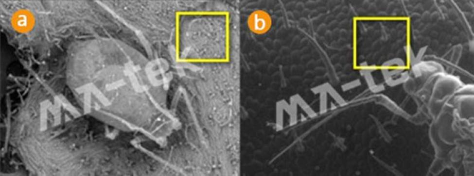
Cooling Stage low temperature observation
Cooling stage must be used in low vacuum mode, and can control the sample temperature at-50°C to 70°C,Through low-temperature environments, the crystallization behavior and phase changes of materials under different temperature conditions can be observed, commonly used in material research and biological sample analysis.
- Ion Channeling Contrast images show the distribution of internal grains and crystal structure in the solder.
- Solder Bump (solder bump, solder ball, or simply bump) microstructure SEM images can observe grain orientation and metal interfaces.
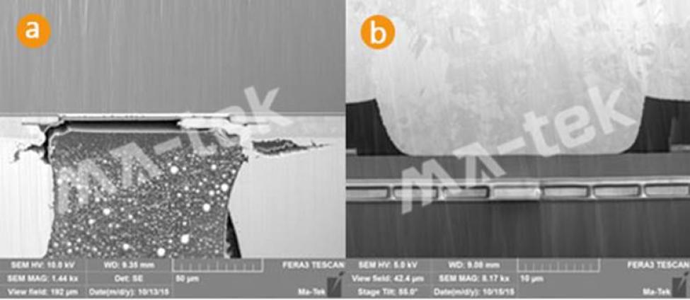
Rocking Stage automatic angle polishing
The rocking stage can automatically rotate the sample angle, making ion beam processing more uniform. Compared to manual angle adjustments, it can effectively reduce cross-section knife marks and improve cross-section quality.
- Manual Polishing cross-sectional imageAfter the sample is manually adjusted at an angle for ion beam polishing, it can be observed that there are still some tool marks or uneven processing traces in the cross-sectional area.
- Rocking Stage automatic rotating polishing cross-section imageBy automatically adjusting the sample angle through the Rocking stage during ion beam processing, knife marks can be effectively reduced and the cross-section flatness improved, making the material interfaces and structural profiles clearer.
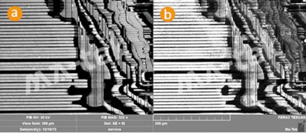
Special Detector
The SI detector can enhance the contrast and three-dimensionality of images, making the material structure and interfaces clearer. In the observation of multilayer metal structures, packaging interconnections, and microstructures, it can effectively strengthen image details and improve material analysis and defect identification capabilities.
-
Secondary Ion Imaging (SI Detector Imaging, Secondary Ion Imaging)The basic image comparison showing the microstructure of the sample allows observation of the material's layered structure and the surface morphology after processing.
-
SI Detector enhances contrast imagesThrough the SI detector, image contrast and three-dimensionality are enhanced, making material interfaces, wire structures, and fine defects clearer.


