
OBIRCH laser beam resistance abnormal detection
IR-OBIRCH (InfraRed Optical Beam Induced Resistance Change)It is a non-destructive failure analysis technique that detects abnormal conduction or leakage locations by scanning the IC surface (or back) with an infrared laser, causing resistance changes through localized heating.OBIRCH is particularly suitable for locating "low-ohm resistance anomalies" and "metal layer defects," often used in conjunction with EMMI or InGaAs as a key cross-validation technique in the FA process.
Compared to photon emission analysis (EMMI), OBIRCH does not rely on the device's own light emission, but actively usesinfrared laser with a wavelength of about 1340 nmScanning the chip, when the scanning point experiences resistance changes due to localized heating, it will cause changes in current or voltage under fixed voltage or current conditions. The system then detects this change signal and locates the defect position.
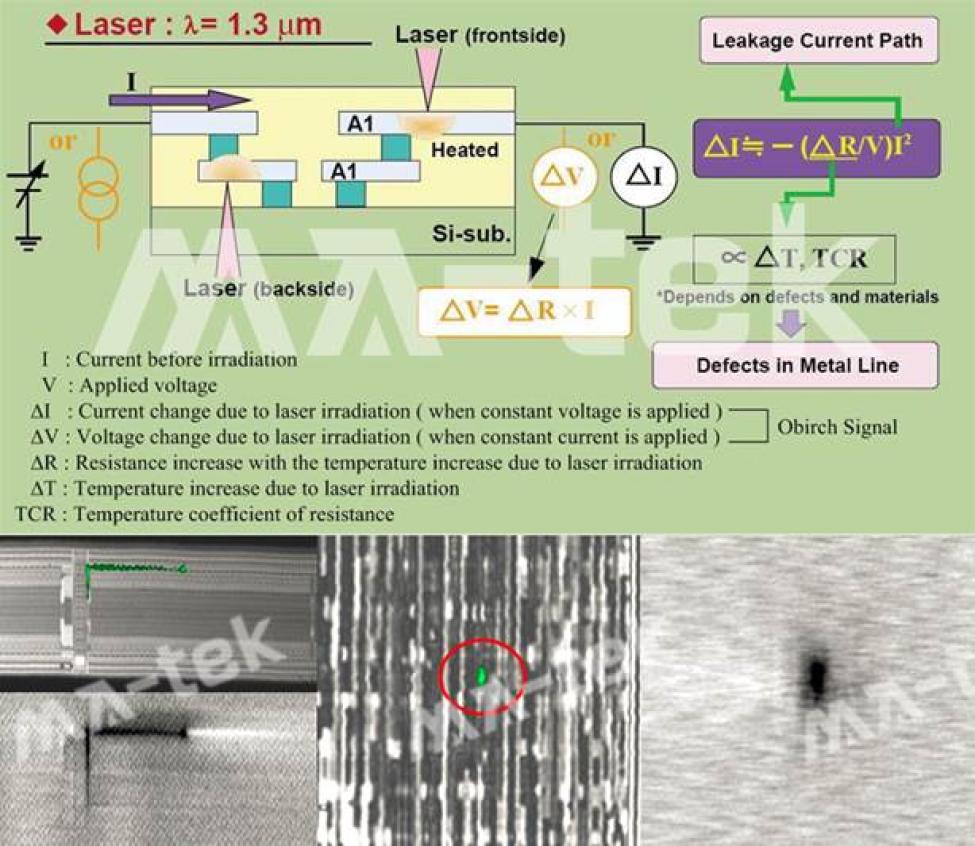
In practical analysis, OBIRCH has a high sensitivity to low-ohm anomalies and can be applied from both the front and back of the chip. OBIRCH can effectively shorten the positioning time and improve the analysis success rate under advanced process nodes, especially suitable for the following situations:
-
Internal cavities or local damage in metal wires
-
Via / Contact Poor Connection
-
Metal or Poly bridging
-
IDDQ static current anomaly
-
Gate oxide leakage
-
ESD and Latch-up Failure
-
Abnormal conduction of components in operation
In advanced process IC failure analysis, a single analysis technique often struggles to fully locate defects. Different types of defects, such asOpen, Short, Leakage or High Resistanceneeds to be combined with different electrical localization techniques for cross-validation.
MA-tekThrough integrationEBIC, EBAC, EBIRCH and OBIRCHAdvanced positioning technologies can quickly identify defect locations for different failure modes, and further confirm the root cause using physical analysis methods such as FIB and TEM.
As the process nodes move towards5nm, 3nm, or even 2nmThe internal structure of the chip has become more complex, and the defect locations are often located in deep metal layers or at the nanoscale junctions.
Through the cross-application of different analysis techniques, it is possible to:
-
Improve defect localization success rate
-
reduce misjudgment
-
shorten analysis time
-
Improve the success rate of subsequent FIB / TEM sample preparation
Therefore, in advanced process failure analysis,EBIC, EBAC, EBIRCH and OBIRCHhas become an indispensable electrical localization tool.
| analysis technology | Main Principle | Applicable defect types | Application |
|---|---|---|---|
| EBIC | The electron beam generates electron-hole pairs and forms a current image. | Junction leakage、Gate oxide breakdown | Interface defect localization, oxide layer breakdown analysis |
| EBAC | Electron beam excites the current in the metal wire and tracks the conduction path. | Metal open、High resistance | Multi-layer metal interconnect open circuit localization |
| EBIRCH | The electron beam causes localized temperature rise leading to resistance changes. | Metal short、High impedance | Metal short circuit and high impedance defects |
| OBIRCH | Laser localized heating causes resistance changes. | Short defect, Leakage path | Packaging and chip short circuit localization |
MA-tek has long been deeply engaged in the field of failure analysis for advanced processes and high-reliability products, constructing a complete one-stop analysis platform through cross-technology integration and professional interpretation capabilities. The OBIRCH technology can seamlessly connect with EMMI, InGaAs, electrical measurement, and FIB repair technology, forming a highly efficient integrated process from anomaly detection, defect localization to subsequent structural repair and physical analysis.
Through systematic technology integration and experience interpretation, the positioning time can be significantly shortened, defect identification accuracy improved, and the success rate of subsequent physical failure analysis (PFA) and root cause determination increased. This assists customers in grasping the core of the problem in the shortest time possible, reducing development and mass production risks. Combining high-resolution infrared laser scanning technology with MA-tek's comprehensive failure analysis integration capabilities, OBIRCH has high sensitivity and success rate positioning advantages for advanced node processes and low ohmic resistance anomalies, particularly suitable for abnormal diagnostics of tiny metal wires, contact holes, and complex multilayer structures.
In the trend of continuous miniaturization of advanced processes and increasingly complex structures, precise and efficient defect localization capability has become a key to competition. MA-tek focuses on an integrated analysis strategy to assist clients in steadily improving product quality and reliability in the competition of advanced technologies, making every failure analysis a key opportunity to optimize processes and strengthen competitiveness.
-
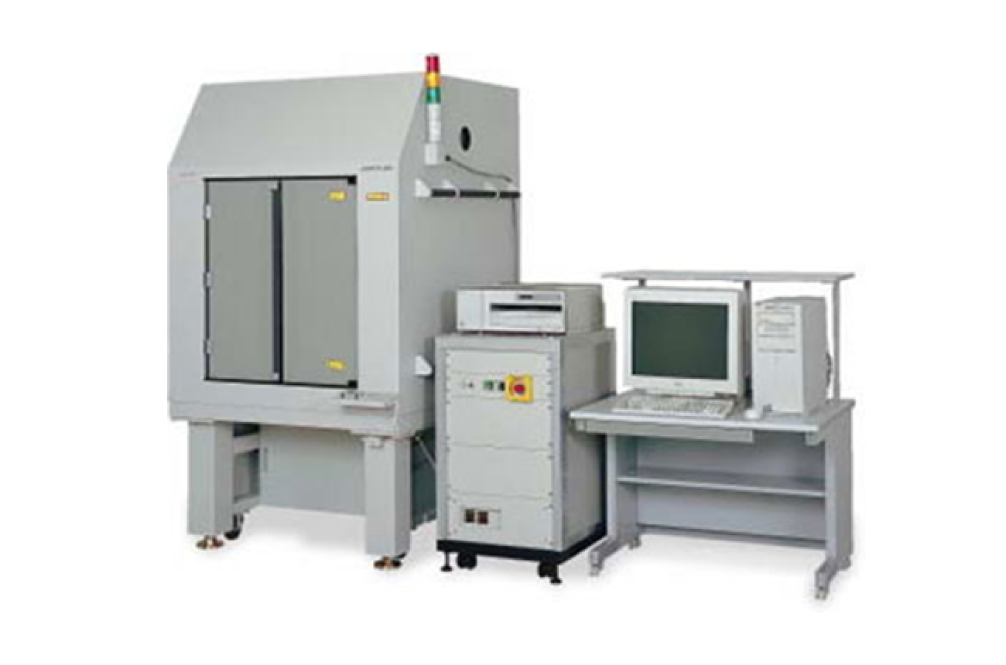 Figure | HAMAMATSU uAMOS-200
 -
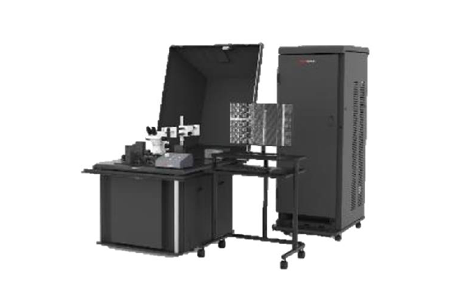 Figure | Meridian S
With the shrinking of processes and the increasing demand for wafer-level analysis, MA-tek has introduced an inverted OBIRCH platform and a high-resolution optical system to further enhance analysis capabilities.
- Inverted Lens Design (Inverted System):The inverted design allows for analysis directly at the wafer level, effectively controlling the range and force of the probe, and solving the issues of poor pad conditions or inability to make connections, significantly improving the timeliness and success rate of the analysis.
- High-resolution SIL lens (Solid Immersion Lens):Through the 350X Solid Immersion Lens (SIL) dedicated lens, the positioning accuracy of advanced process nodes can be improved, allowing for accurate identification of resistance anomaly locations even in extremely fine metal wires or contact hole structures. It demonstrates significant advantages for advanced process nodes greater than 3nm.
- New Active Probe technology and high-performance amplifiers:The OBIRCH system can effectively enhance the detection capability of low ohm signals, reduce external noise interference, and even analyze resistance anomalies below 20 Ω, which is particularly critical for identifying small metal defects in advanced processes.
- Integrating advanced analysis technology:The system can integrate C-AFM, Nanoprobing, and circuit editing technologies to improve the success rate of TEM sample preparation and reduce new wire costs, fully optimizing the success rate of PFA (Physical Failure Analysis) and the overall process efficiency in advanced manufacturing.


