
Thermal EMMI
Thermal EMMI (Thermal Emission Microscopy) is a highly sensitive failure analysis technique for defect localization by detecting the minute thermal radiation generated by components in an energized state. Compared to traditional photon emission analysis (EMMI) that detects photon signals, Thermal EMMI detects the infrared thermal radiation distribution caused by abnormal conduction, leakage, or localized short circuits in the components. This technology allows for localization directly from the front or back of the IC without opening the package, quickly determining whether the heat source issue belongs to the chip itself or the packaging structure, making it a highly non-destructive analysis tool. For advanced packaging, stacked chips, and large-area products, Thermal EMMI demonstrates unique advantages.
MA-tekLong-term focus on advanced process and packaging level failure analysis, equipped with complete technical integration capabilities such as Thermal EMMI, PEM-CCD, InGaAs, OBIRCH, and electrical measurements. Through cross-technical platform collaboration and professional interpretation experience, the best positioning tools can be selected according to failure modes, effectively shortening positioning time, improving defect identification accuracy, and enhancing the success rate of subsequent physical failure analysis (PFA).
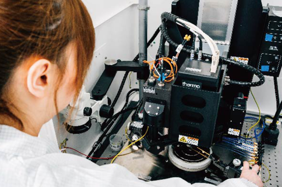
Thermo ELITE Advanced Thermal Emission Analysis System
Thermo ELITE is a high-performance Thermal Emission analysis platform, suitable for high voltage, high current, and power component applications.
The system is suitable for the analysis of power components and large area module products, with the main technical specifications including:
-
Voltage range: ±3000V (@100mA)
-
Current range: 3A (@40V)
-
Frequency range: 1Hz–89Hz
-
Wide-angle field of view: 30cm × 30cm
-
Lens options: WA, 1X, 10X, LSM20X, LSM50X
-
Support for back-side probing and image stitching technology
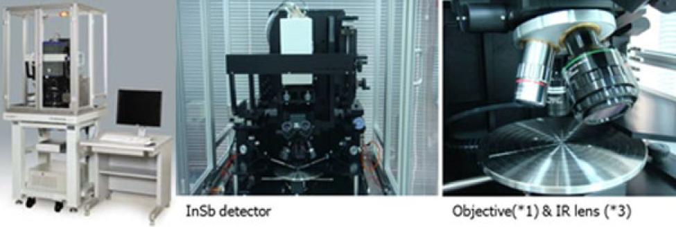
HAMAMATSU THEMOS mini
THEMOS mini is a compact and highly sensitive thermal localization device that can quickly locate defect positions through the front or back of the IC, making it particularly suitable for analysis scenarios with limited space or rapid assessment needs.
Thermal EMMI has extremely high sensitivity thermal source detection capability in the market, achieving a temperature resolution of <1 mK within seconds, and can even measure stably for long periods down to <10 µK. Through real-time locking measurement technology, it significantly enhances the signal-to-noise ratio, making small abnormal thermal sources clearer. The technology supports both static and dynamic analysis modes, allowing observation of component thermal distribution changes under actual operating conditions, particularly suitable for application state verification during the product development phase.
Through the thermal source depth reading capability, it can distinguish whether the defect is located at the chip body or packaging level, assisting in quickly narrowing down the scope of subsequent destructive analysis. Thermal EMMI can be widely applied to:
-
Abnormal resistance of metal contact holes (Via / Contact)
-
Stacked Die and packaging wire bonding anomalies
-
PCB traces defects or short circuits
-
Dielectric layer breakdown and leakage current
-
TFT-LCD or Organic EL leakage localization
-
ESD and Latch-up Failure Analysis
-
Analysis of Abnormal Heating in Power Components
-
Large area product (PCB, panel, passive components) thermal source localization
-
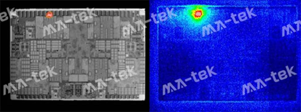 Image | Comparison of IC backside image and thermal imageThe left image shows the structure of the IC back, and the right image shows the corresponding thermal radiation image. The red area indicates the location of abnormal heat sources, which can be accurately matched to the circuit area, significantly reducing the fault localization time.
 -
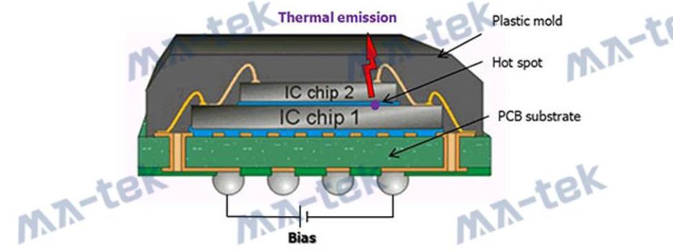 Image | Front-side thermal radiation analysis of ICDirect thermal radiation measurement on the front side of the IC is suitable for samples that have not undergone back-side processing. When electrical anomalies cause local leakage or short circuits, hotspot images can be formed in real-time to assist in quickly determining the failure area.
-
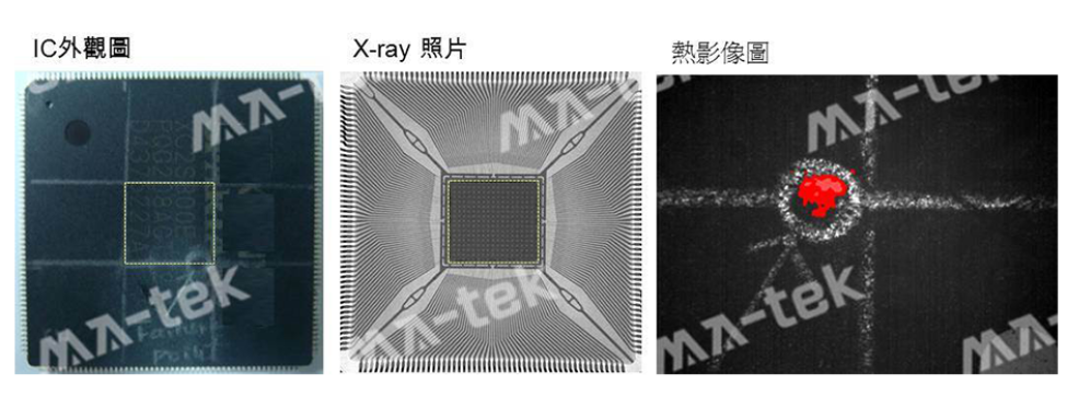 Figure | IC Appearance Diagram / X-ray Photo / Thermal ImageIntegrating appearance images, X-ray internal structure inspection, and thermal radiation images allows for multi-level cross-comparison analysis. By overlaying structural and thermal signals, it accurately determines the defect location and possible causes.
 -
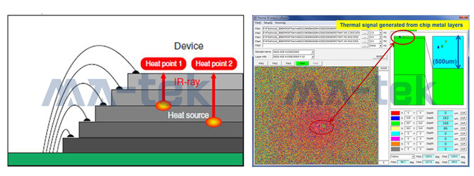 Image | Thermal Source Depth Estimation AnalysisThrough frequency and phase modulation analysis, the depth position of the heat source within the chip can be estimated. Different frequencies correspond to different thermal diffusion depths, which helps in determining defect layers, especially suitable for stacked die and multilayer metal structure analysis.
-
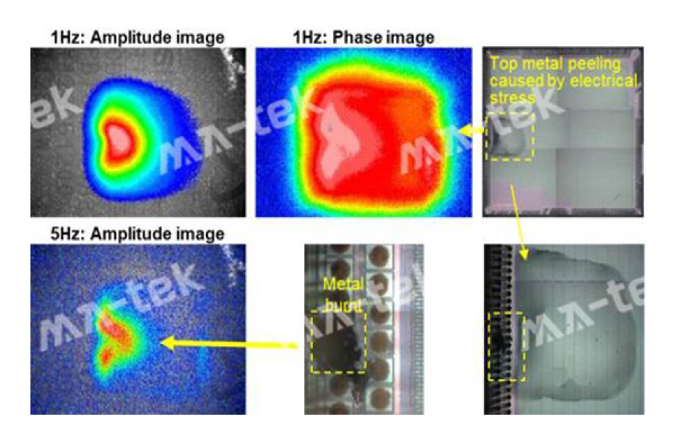 Figure | Correspondence of Multi-frequency Amplitude and Phase
The amplitude and phase images at different modulation frequencies (1Hz / 5Hz) can enhance the ability to identify weak thermal signals. The analysis results correspond closely with the height of actual metal layer delamination defects, confirming the precise positioning capability of Lock-in Thermal Emission technology.
-
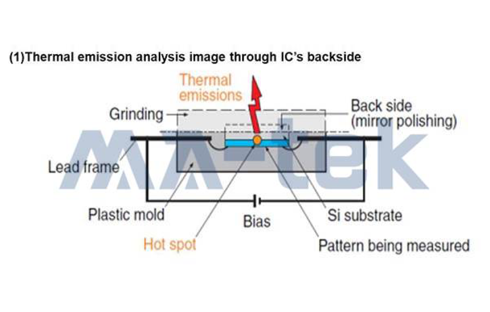 Image | IC backside thermal radiation analysisThrough IC back grinding and mirror polishing treatment, infrared thermal radiation signals generated by defects are detected under powered bias conditions. Hot spots can penetrate the silicon substrate and be captured by high-sensitivity infrared detectors, achieving non-destructive failure localization.
Thermal EMMI utilizes high-sensitivityInSb (Indium Antimonide) infrared detectorMeasure the thermal radiation distribution generated by the component while powered on. When there is leakage, local short circuits, or abnormal contact impedance inside the chip, a slight temperature increase (ΔT) occurs in that area. Through a high-resolution infrared imaging system, these thermal source distributions can be converted into visual thermal images. The Lock-in technique enhances the signal-to-noise ratio, allowing even very small temperature differences to be identified. In addition to planar positioning, Thermal EMMI can also estimate the depth position of thermal sources through thermal diffusion characteristics, which is particularly important for multi-layer packaging and stacked chip analysis.
The system can locate defects without opening the device, effectively shortening the analysis process and reducing sample risk. For cases where the defect location on the chip or packaging is not yet determined, a preliminary distinction can be made quickly. Its thermal source depth reading capability allows analysts to assess whether the defect is located in stacked chips, packaging wire bonds, or PCB traces, avoiding unnecessary destructive cutting.
Thermal EMMI is not only applicable to ICs, but also demonstrates its advantages of high stability and wide measurement range under power components and high voltage testing conditions, applicable to:
-
Large Area Thermal Anomaly Analysis of PCB
-
Leakage detection for panels and displays
-
Passive components and module products
-
Power components and high current application products


