
EELS Electron Energy Loss Spectrum
Electron Energy Loss Spectroscopy (EELS)EELSis a high-resolution material analysis technique that combines transmission electron microscopy (TEM) or scanning transmission electron microscopy (STEM). EELS mainly analyzes the energy loss generated after measuring the electron beam passing through the sample.Energy Loss to analyze the elemental composition and electronic structure of materials. When a high-energy electron beam passes through the sample, some electrons undergo inelastic scattering with the atoms in the sample, resulting in a decrease in electron energy. By analyzing the magnitude of the electron energy loss and the positions of the characteristic peaks, information about the types of elements, chemical bonding, and electronic structure in the material can be obtained.
EELS is particularly suitable forLow atomic number elementsthe analysis, such as: carbon (C), nitrogen (N), oxygen (O), boron (B), its energy resolution can reachabout 1 eV, combined with scanning transmission electron microscopy (STEM) at approximately 1 nm spatial resolutionmaking EELS an important tool for nanoscale material research and semiconductor process analysis.
Electron Energy Loss Spectroscopy (EELS) is a High-order component analysis detection instrument installed under a transmission electron microscope (TEM)When a high-energy electron beam penetrates the sample, it interacts with the electrons in the material's atoms.Inelastic Scattering , leading to a specific degree of energy loss for the incident electrons.
When the electron beam interacts with the atoms in the material, it may exciteCore Electrons or Valence Electronsto cause the electron beam to lose corresponding energy, by measuring and analyzing the distribution of these electron energy losses, important information about the material at the nanoscale or even atomic scale can be obtained, includingelement types, chemical bonding states, electronic structure, and band structure, etc.
In addition, EELS can also be combined withEnergy Filtered TEM (EFTEM, Energy Filtered Imaging)The technology effectively enhances image contrast by selecting electrons within a specific energy range to form images, and is used to observe the spatial distribution of specific elements or chemical states within the sample, significantly improving the analytical capability of material composition and structure.
In EELS spectra, it can usually be divided into two main analysis regions:
-
Low-loss region
-
Plasmon energy
-
band structure
-
Dielectric properties of materials
-
-
Core-loss region
-
element characteristic energy peak
-
Chemical bonding information
-
atomic electronic structure
-
In electron microscopy material analysis, electron energy loss spectroscopy (EELS) and energy dispersive X-ray spectroscopy (EDS / EDX) are both commonly used elemental analysis techniques, which can be combined with TEM or SEM for material composition analysis. However, their analysis principles and applicable situations differ, and in practice, these two techniques are usuallycomplementary useto obtain more complete material information.
EDS mainly generates from the excitation of the sample by the electron beam.Characteristic X-rayto determine the elemental composition in materials, making it very suitable for the rapid identification of the types and distribution of elements present in the materials; while EELS measures the energy loss generated after electrons penetrate the sample.energy loss signalIn addition to elemental information, it can further analyze.Chemical bonding, oxidation state, and electronic structureto explore deeper material properties.
In addition, EELS has advantages in energy resolution and nanoscale analysis capabilities, with energy resolution reachingabout 1 eV or lowerIt can effectively distinguish overlapping element signals that are difficult to resolve with EDS, such as the signal interference of common elements in semiconductor materials.
| Analysis Items |
EELS |
EDS |
|---|---|---|
| Analysis Principle | Measuring the energy loss of electrons after penetrating the sample | Measure the characteristic X-ray emitted by the sample |
| Main equipment | TEM / STEM | SEM / TEM |
| energy resolution | about 1 eV or better | about several eV |
| spatial resolution | nano or even atomic scale | nanometer scale |
| Suitable elements | Low atomic number elements (C, N, O, B) | Middle to high atomic number elements |
| suitable elements | Nanomaterials and chemical state analysis | Element composition and element distribution |
| Common Uses | Nanomaterials and Chemical State Analysis | Qualitative and quantitative analysis of elements |
In practical materials analysis, EELS and EDS are usuallyused in conjunctionfor example, in the analysis of semiconductor materials or nanomaterials,EDSCan quickly confirm the elemental composition of materials;EELSchemical states and electronic structures of elements can be further analyzed. Through the integration of the two techniques, a more complete understanding of the materials can be achieved.Element composition, chemical bonding, and nanoscale structural characteristicsIt has important value for advanced semiconductor processes and nanomaterial research.
MA-tek has a completeTEM / STEM / EELS integrated analysis platformelement and chemical bond analysis at the nanoscale for advanced materials and semiconductor process structures. Through high-resolution energy analysis systems and professional data analysis capabilities, it can deeply analyze the materials.element distribution, chemical bond state and electronic structureproviding highly reliable information on the microstructure of materials, EELS analysis has extremely high value in the research of nanomaterials due to its capabilities.High energy resolution, high spatial resolution, and high sensitivity to low atomic number elements.can analyze the distribution and chemical states of elements such as carbon, nitrogen, and oxygen, and perform precise element mapping and chemical bond interpretation at the nanoscale, MA-tek can throughSTEM-EELS scanning analysis and Energy-Filtered TEM technologyto establish the composition and electronic structure distribution of materials at the nanoscale, and can be applied to advanced semiconductor process materials and nanomaterials research.
-
Advanced materials and semiconductor process analysis capabilities
Through STEM line scan and element mapping technologyMA-tek's EELS technology can be applied to various advanced material analysis needs, analyzing material composition distribution and interface structure at the nanoscale and even close to the atomic scale, which has critical value for advanced processes and material development.-
semiconductorGate oxide layer and low dielectric materials (Low-k) analysis
-
Nano thin film materials and interface chemical analysis
-
Metal oxides and chemical bond analysis
-
Element distribution and nanoscale composition variation analysis
-
Band structure and electronic structure research
-
-
One-stop material analysis service with multi-technology integration
MA-tek has the capability of material analysis through cross-technology integration, which can combineEELS and high-resolution imaging observation of TEM, EDX, and STEMCombine, assist customersAnalyze the correlation between material structure and processes, enhance product reliability and process optimization efficiency.and provide high-reliability nano material analysis services-
Microstructure of materials
-
element composition distribution
-
chemical bonding state
-
nanometer-scale interface structure
-
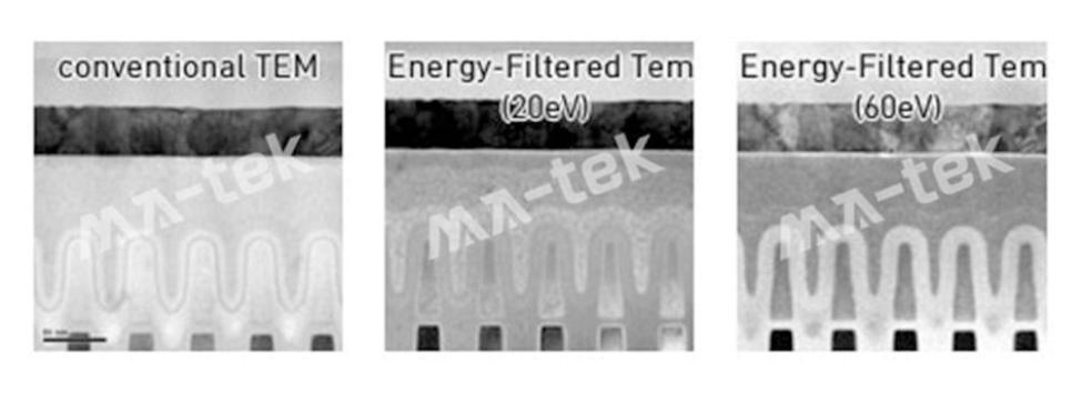
Energy-filtered imaging to observe structural differences in materials.
Using Energy Filtered TEM technology, by selecting electron signals from different energy ranges, the contrast changes in the material structure can be observed. Under different energy filtering conditions, the internal structure and element distribution of the material will present different imaging characteristics.
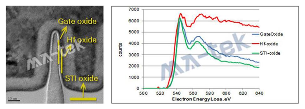
Chemical bonding and oxidation state analysis
Using EELSNear Edge Fine Structure(ELNES)Analysis can identify different chemical bond states. The image shows the differences in the oxygen element energy spectrum of the gate oxide layer in a 16 nm semiconductor process FinFET, thereby distinguishing different oxide materials.
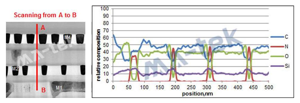
Nano-scale element distribution analysis
Combining STEM scanning with EELS spectrum analysis, line scanning can be performed along a specified path to obtain nanoscale variations in element concentration within the material, commonly used for the analysis of low dielectric materials or multilayer thin film materials in semiconductors.
EDX: Element composition
EELS: Element + Chemical bonding + Electronic structure


