
UV-OM fluorescence microscope
In semiconductor packaging and electronic component analysis, the presence of tiny gaps or leakage issues at the packaging interface often affects the reliability and long-term lifespan of the components. However, for chip-scale packaging or small-sized components, traditional red ink penetration tests often struggle to clearly identify leakage paths under a microscope.
Fluorescence microscopeBy combining fluorescent penetration experiments, the characteristics of fluorescent agents that produce obvious luminescent signals under ultraviolet light allow even very small amounts of penetration to be clearly identified. Through UV light sources and microscopic observation, the locations of packaging joint gaps, cracks, or material leaks can be quickly located. This is commonly applied in: semiconductor packaging leak detection, IC packaging joint interface defect observation, LED phosphor distribution analysis, detection of small packaging cracks and gaps, and reliability analysis of electronic component packaging.
Fluorescence microscopy analysis mainly utilizes fluorescence penetration testing (FPI)Fluorescent Penetrant Inspection, FPIDefect observation is conducted. During the measurement process, the sample is first immersed in a fluorescent penetrant under vacuum conditions, allowing the fluorescent agent to seep into the tiny gaps or cracks in the packaging interface. When the sample is exposed to ultraviolet light (UV Light), the fluorescent agent that has penetrated the defect location emits a distinct fluorescent signal. Due to the significant contrast between the fluorescent brightness and the background, even extremely small amounts of penetration can be clearly identified, enabling engineers to quickly locate packaging leaks or bonding defect positions.
The method primarily utilizes the ability of fluorescent dyes to penetrate tiny cracks or pores on the surface of materials, generating a significant fluorescent signal under ultraviolet (UV) light to assist in observing and locating defect positions. This method has high sensitivity and can effectively detect fine cracks, pores, or packaging joint gaps that are difficult to identify with the naked eye, thus it is widely applied in fields such as semiconductor packaging, electronic components, metal materials, and reliability analysis.
In semiconductor packaging analysis, fluorescence penetration testing is often used to detect whether there are leakage or bonding issues at the packaging interface. When the fluorescent penetrant enters the tiny gaps on the surface of the sample, it emits a noticeable fluorescence under ultraviolet light, creating a strong contrast between the defect location and the background. Engineers can quickly observe and determine the defect location through the fluorescence microscope (UV-OM).
Fluorescent penetration experiments typically include the following steps:
- Sample pretreatment (Cleaning):Before conducting the inspection, the surface of the sample must be cleaned to remove oil, dust, or other contaminants to avoid affecting the fluorescence penetration effect.
- Fluorescent Penetration:Immerse the sample in the fluorescent penetrant, and it can be done in a vacuum environment, making it easier for the fluorescent agent to penetrate the tiny cracks or gaps on the material's surface.
- Remove excess penetrant from the surface (Cleaning / Rinse):Remove excess fluorescent liquid from the sample surface to avoid background fluorescence interference during observation.
- UV Inspection:Using ultraviolet light to irradiate the sample, the fluorescent agent that infiltrates the defects will emit bright light, allowing engineers to observe the distribution of fluorescence through a fluorescence microscope and determine the defect location and leakage path.
| technology | Main light source | Main Uses |
|---|---|---|
| OM optical microscope | visible light | Surface structure and packaging appearance observation |
| UV-OM fluorescence microscope | ultraviolet light | Fluorescent Leakage and Material Distribution Analysis |
| IR-OMInfrared Optical Microscope | Infrared light | Observation of internal structure of the chip |
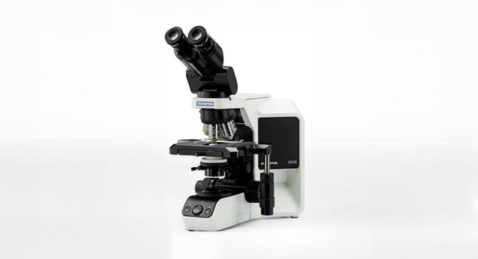
MA-tekLong-term focus on semiconductor material analysis and failure analysis, establishing a complete packaging analysis and material testing platform. In the field of fluorescence microscopy analysis, MA-tek can combine multiple analytical techniques to provide a more comprehensive packaging defect assessment capability, through integration:
-
UV-OM fluorescence microscopy observation
-
X-ray packaging inspection
-
SEM microstructure analysis
-
FIB cross-section sample preparation
-
EDX material composition analysis
This can form, from Packaging defect detection → Microstructure analysis → Material root cause analysisthe complete analysis process, assisting customers in quickly clarifying the reasons for packaging anomalies and improving product reliability.
- Package leakage detection
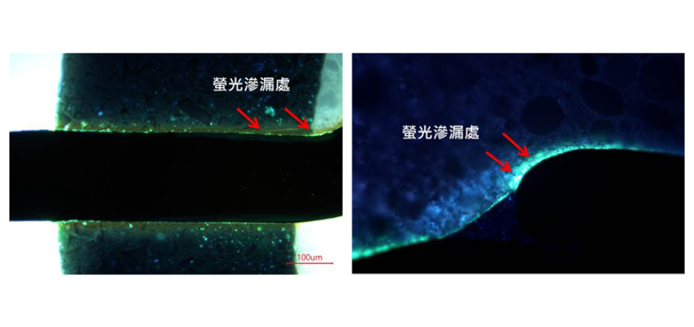
UV-OM observes the location of package leakage.
When there are tiny cracks or bonding defects in the packaging structure, the fluorescent agent will seep into the material along the gaps. Under ultraviolet light, the leakage locations will show obvious fluorescent spots, allowing engineers to quickly locate the abnormal areas of the packaging. For example, when there are abnormalities in the packaging paddle or packaging interface, UV-OM can effectively observe the fluorescent leakage and determine the defect location. - Observation of LED phosphor distribution
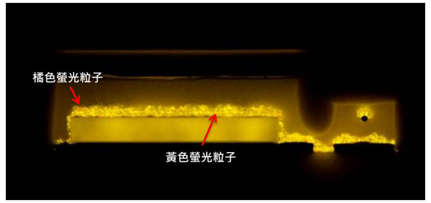
LED phosphor distribution observation
In LED packaging, the distribution of phosphor particles affects luminous efficiency and color uniformity. Through UV-OM fluorescence microscopy, the distribution and composition of different phosphor particles can be clearly identified, assisting engineers in analyzing the quality of fluorescent materials and packaging uniformity.


