
IC packaging wire bonding service
Wire BondingIt is an important technology for establishing electrical connections between the die and external circuits or package pins. Through precise wire bonding equipment and process control, gold wires, copper wires, or aluminum wires can be bonded to the bond pads and package pins, allowing signals to be transmitted between the chip and external circuits. MA-tek provides complete IC packaging wire bonding services.IC packaging wire bonding servicesupporting research and development testing, failure analysis (FA), reliability verification (RA), and packaging development needs, assisting customers in quickly completing chip packaging and functional verification.
Wire bonding is a key process for establishing electrical connections between the die and the package pins. Depending on the wire material and process method, it can be mainly divided into two types of wire bonding:
-
Ball Bonding
Using gold wire (Au wire) or copper wire (Cu wire) for wire bonding. First, an arc is used to form a metal ball (Free Air Ball), then the metal ball is pressed onto the pad to form the first bond (1st bond), and afterward, the wire is shaped into an arc to complete the second bond (2nd bond). -
Wedge Bonding
Using aluminum wire (Al wire) for bonding, a wedge tool is used to directly press and form the solder joint, commonly applied in power components or special packaging requirements.
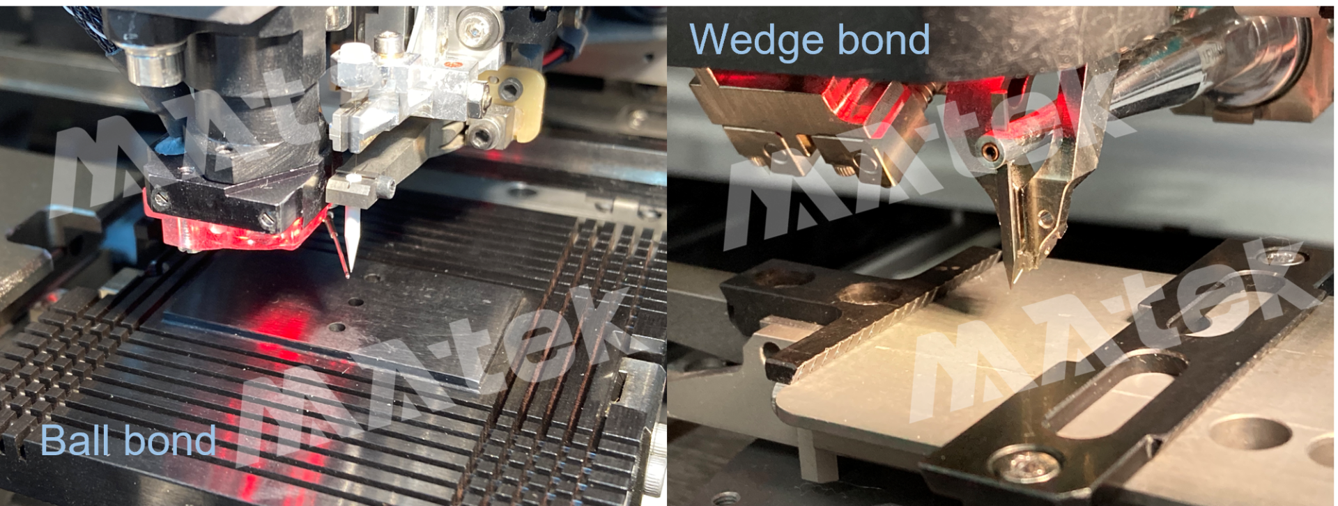 Figure | (a) Ball bonding (gold wire & copper wire) (b) Wedge bonding (aluminum wire)
By precisely controlling the welding temperature, pressure, and ultrasonic energy, good conductivity and mechanical strength of the solder joint can be ensured.
Wire bonding technology is widely used in:
-
Chip-on-board (COB)
-
Die stacking packaging
-
PCB chip-on-board connection
-
High pin count IC packaging
-
COF / COG display components re-soldering
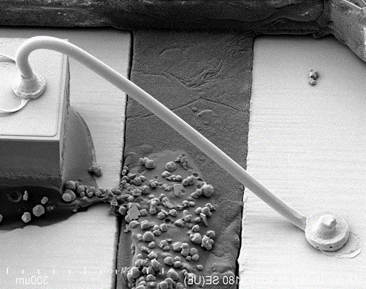 Diagram | Wire Bonding Process Schematic
The wire bonding process involves the formation of the ball bond, the first bond, the formation of the wire arc, and the completion of the second bond, establishing the electrical connection between the die and the package. The precise bonding from the formation of the ball bond to the completion of the second bond typically includes the following steps:
-
Free Air Ball formation:Metal balls are formed through arc discharge.
-
1st Bond: Join the metal ball to the chip solder pad.
-
Looping (arc formation):Control the wire height and arc shape.
-
2nd Bond: Solder wire bonding to the package pins or substrate.
MA-tek not only provides packaging and wire bonding services, but also integrates complete material analysis and failure analysis capabilities, offering integrated services for semiconductor research and development as well as problem resolution. Through the integration of comprehensive packaging and analysis technologies, MA-tek can assist customers in accelerating product development and problem diagnosis, providing highly efficient and reliable semiconductor technology services.
-
High precision fine pitch wire bonding capability (22 μm pitch)
-
Support for various wire materials and packaging forms
-
Provides flexible packaging service delivery, supporting R&D projects and urgent testing needs.
-
Regular items: 5 working days
-
Urgent: 3 working days
-
Urgent items: 1 working day
-
-
Packaging, analysis, and reliability testing integrated services
Important support for packaging development, reliability verification, and failure analysis, MA-tek's IC packaging and wire bonding services can support various research and analysis needs, including:
-
Rapid Packaging (Prototype Packaging)
Support rapid packaging of R&D samples. -
Electrical Verification
Verify the electrical functions after chip packaging.
-
Die Attach
Fix the chip to the packaging substrate or test board. -
Gold wire / Copper wire / Aluminum wire bonding
Complete the electrical connection between the die and the package pins.
-
Die Saw
Cut the wafer into individual chips. -
Wire Bond Pull / Shear Test
Evaluate solder joint strength and reliability. -
SEM / X-ray inspection
Check packaging quality and solder joint structure.
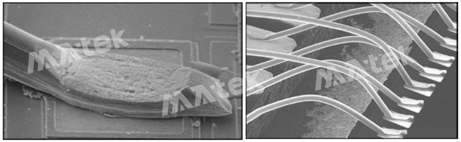 Image | Aluminum wire bonding at 50um pitch (linear)
-
Minimum pitch of gold wire:22 μm
-
Gold wire diameter:0.5 mil
-
Aluminum wire pitch:50 μm
-
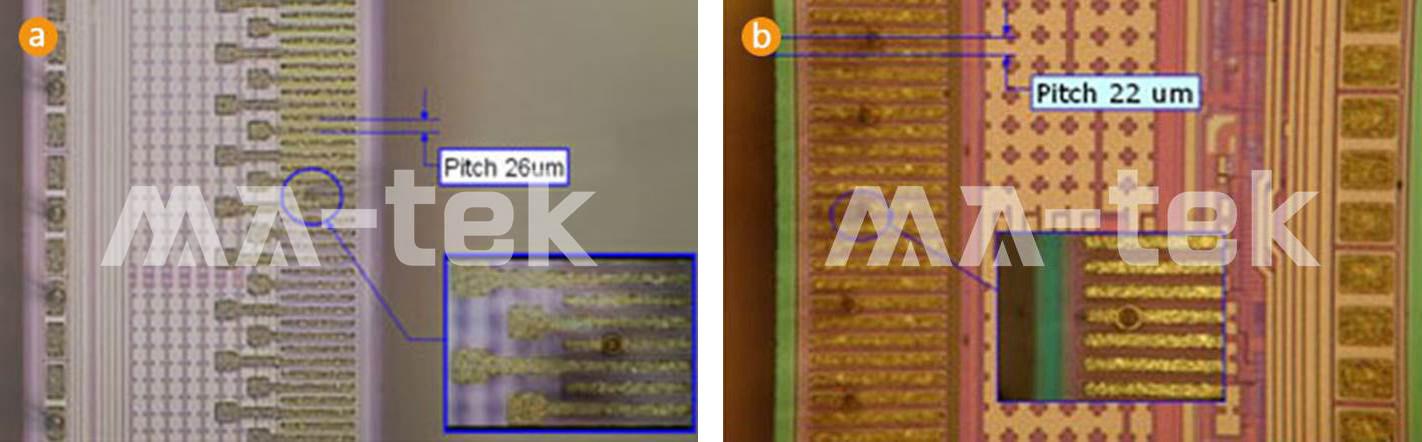
Figure | (a) Optical photo of the product with a 26um gold bump pitch * Gold wire diameter = 0.5 mil
(b) Optical photo of the product with a 22um pitch gold bump.* Gold wire diameter = 0.5 mil
-
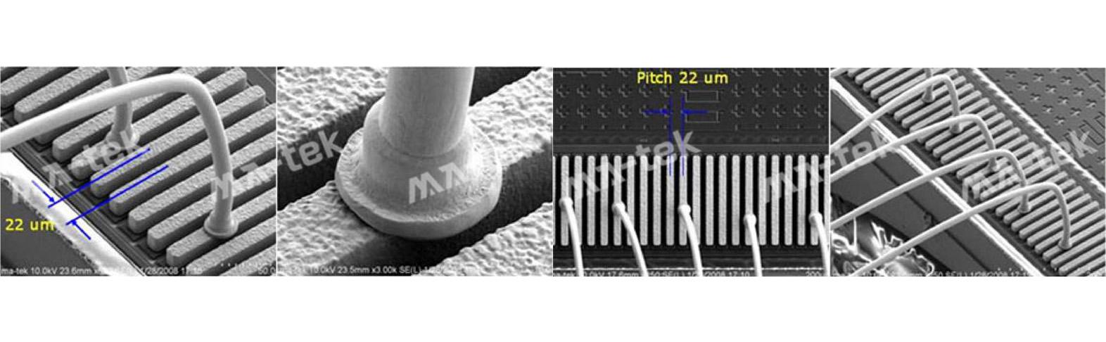
Image | Scanning electron microscope photo of products with a 22um gold bump pitch.
* Gold wire diameter = 0.5 mil
MA-tek can provide variousChip-on-Board (COB)Packaging design, including
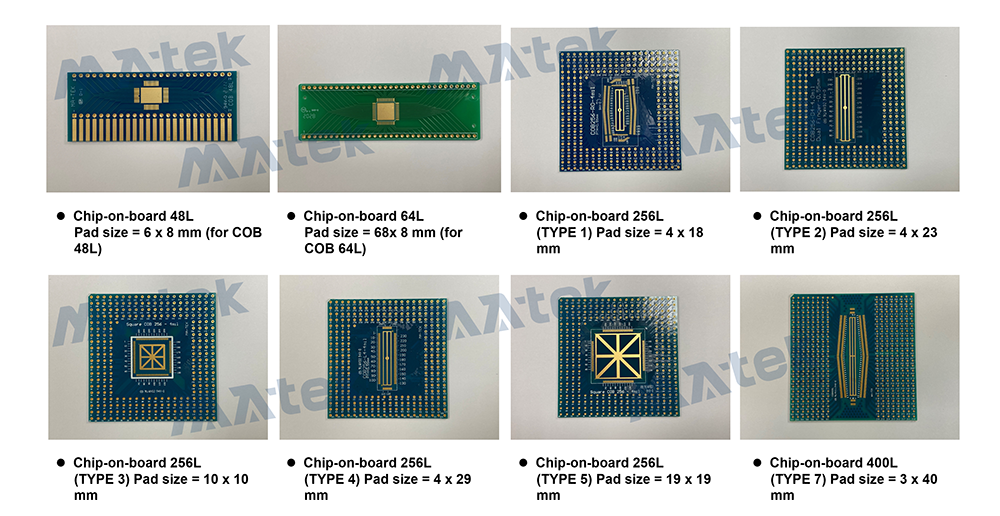
COB packaging can directly encapsulate chips onto the substrate, suitable for R&D testing and high pin count packaging applications. MA-tek supports various Chip-on-Board packaging types and can provide multiple options.Chip-on-Board (COB)Packaging design, including:
-
COB 48L
-
COB 64L
-
COB 256L
-
COB 400L
-
COB materials can be selected as back-side & front-side or with and without bonding.
In addition to COB packaging, MA-tek can also provide various types of ceramic packaging, which can be selected based on the customer's testing requirements:
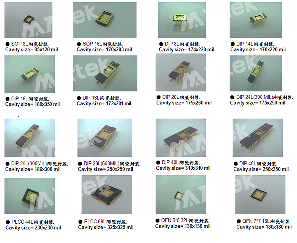

MA-tek provides various chip protection methods, and different cover forms can be chosen after packaging is completed:
-
Epoxy Encapsulation
-
Glass Lid
-
Metal Lid
-
Plastic Lid
Gold wire: 0.5 mil / 0.6 mil / 0.7 mil / 0.8 mil / 1.0 mil / 1.2 mil
Copper wire: 0.8 mil / 1.0 mil / 1.2 mil
Aluminum wire: 0.7 mil / 1.0 mil / 1.2 mil


