
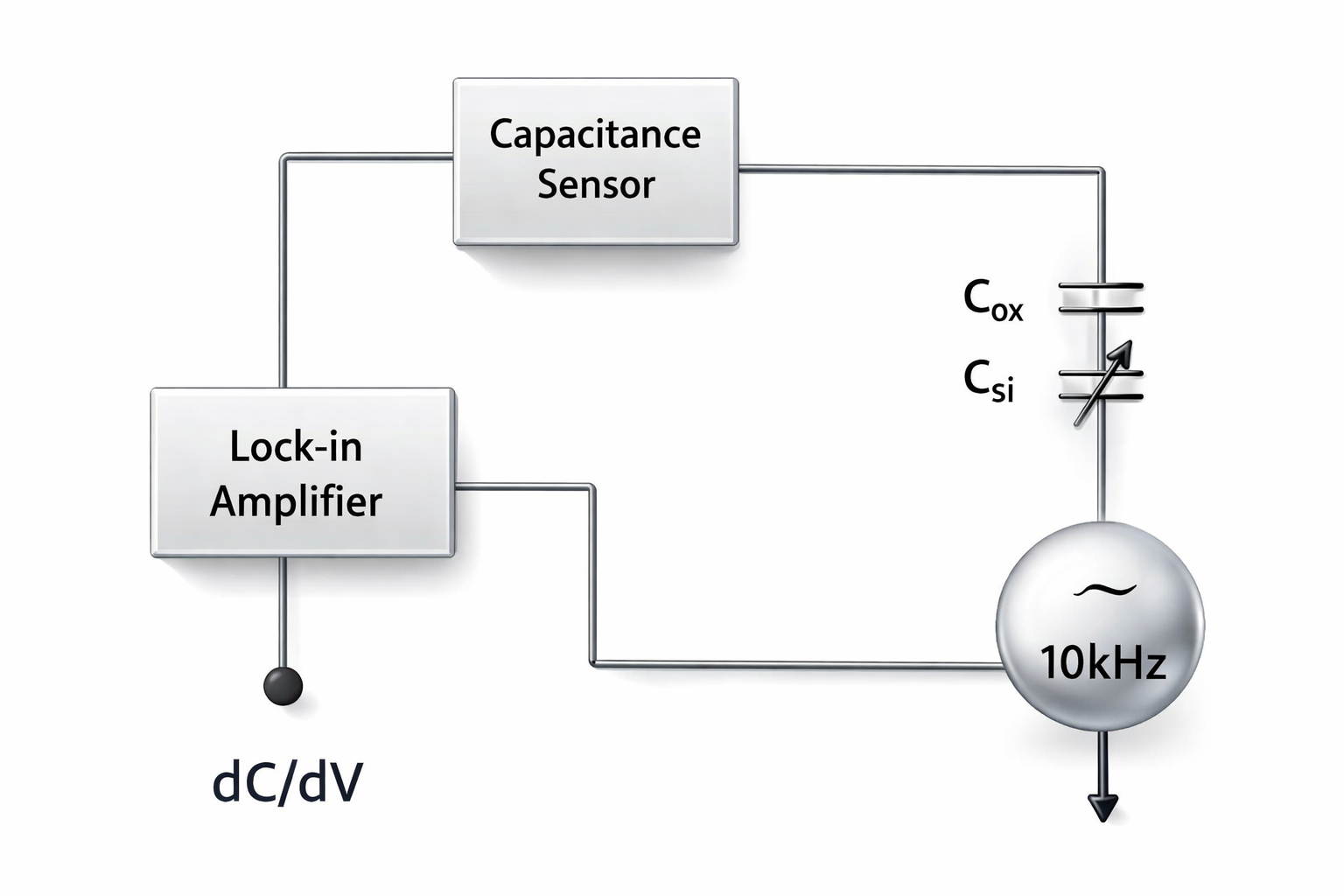
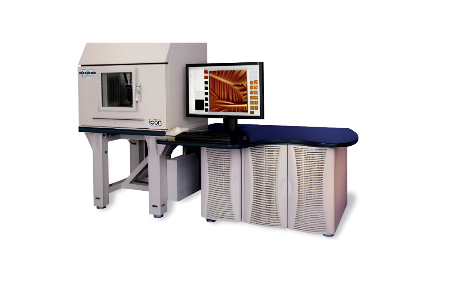
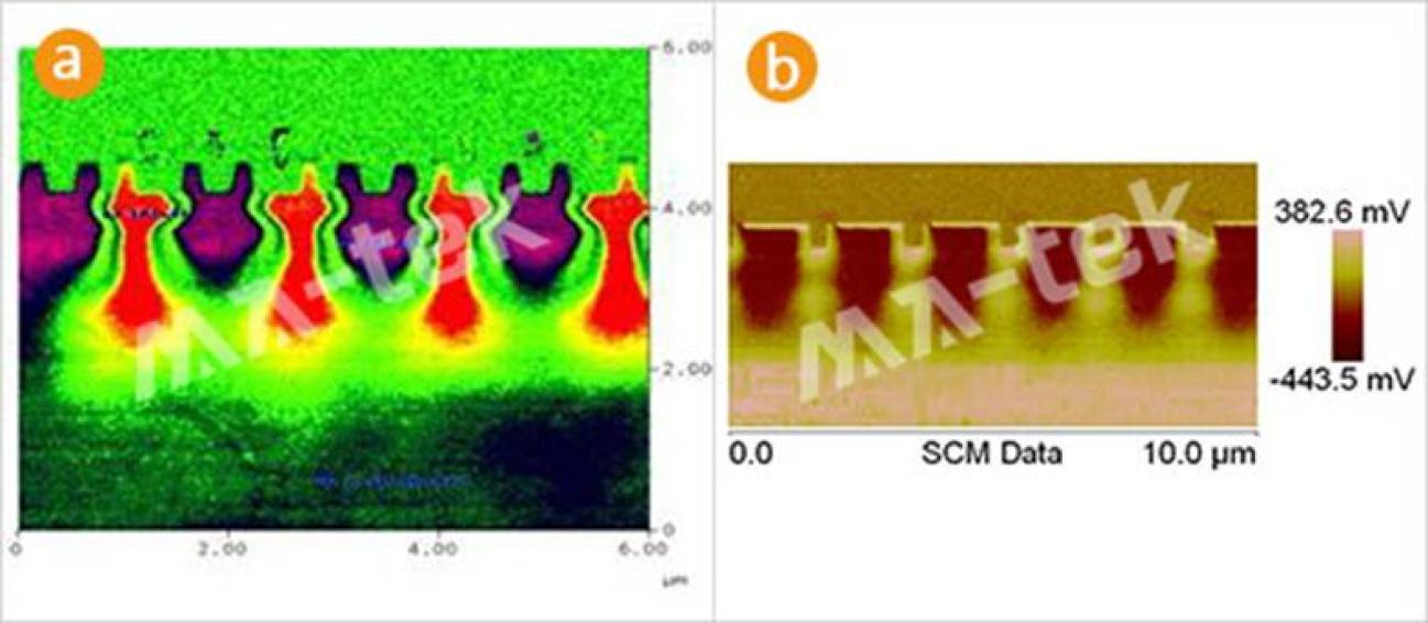
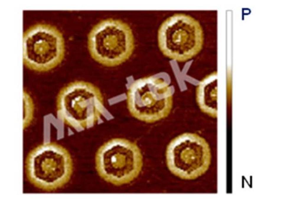
This image isScanning Capacitance Microscopy (SCM) measurements obtained trench structure planar doping distribution images.Through measurementdC/dV signaland converted into images, presenting different areas of the component surface.Doping types and distribution conditions。
The grayscale in the image corresponds to the doping types of the materials, among which:
-
bright areas represents P-type doping region
-
dark areas represents N-type doping region
The high-resolution two-dimensional doping images from SCM allow for clear observation.Doping distribution around the trench structure and junction morphologyhelps in analyzing component structure design, process uniformity, and potential defects.
This analysis technique is commonly applied to:
-
Advanced semiconductor device doping distribution analysis
-
P-N junction structure observation
-
Analysis of process anomalies or leakage issues
-
IC structure reverse engineering analysis


