
EBSD Electron Backscatter Diffraction
Electron Backscatter Diffraction (EBSDis an important microscopic analysis technique that uses electron diffraction signals to analyze the crystal structure and grain orientation of materials. It is widely used in the microscopic structure research of semiconductors, metallic materials, and advanced functional materials. Through EBSD technology, it is possible to analyze the crystal orientation, grain boundary characteristics, and texture distribution of materials at the micron or even sub-micron scale, making it a highly valuable structural analysis tool in materials science and failure analysis.
EBSD detectors are usually installed onScanning Electron Microscope (SEM) or FIB-SEM dual beam systemDuring measurement, the sample surface is usually tilted relative to the electron beam by about70°When a high-energy electron beam strikes the surface of the sample, some electrons will be scattered.Backscattered Electronsbounces off the sample in the form of diffraction when passing through the crystal lattice, forming specific geometric features on the fluorescent screen.Kikuchi Lines and Kikuchi Pattern。
These diffraction patterns carry important information about the crystal structure and grain orientation. By indexing and analyzing the diffraction patterns using EBSD-specific software, an orientation map of the grain orientation distribution at various positions on the sample surface can be established, thereby fully presenting the material's microcrystalline structure.
After obtaining the grain orientation information of various regions of the sample, EBSD can be further used to analyze multiple key material characteristics, includingGrain boundary characteristics, crystal orientation, texture, and local strain distributionThese pieces of information are significant for understanding the mechanisms of material deformation, the effects of processing, and the evolution of microstructures.
In addition, EBSD is often used withEnergy Dispersive X-ray Spectroscopy (EDX)integrated analysis, simultaneously analyzing elemental composition while obtaining crystallographic information, thus completingPhase Identification and Phase Distribution AnalysisBy cross-referencing crystallographic structure and elemental information, the integrity and accuracy of material microstructure analysis can be significantly enhanced.
The basic principle of EBSD (Electron Backscatter Diffraction) is to analyze the crystallographic characteristics of materials using the diffraction phenomenon between the electron beam and the crystal structure. When the electron beam irradiates the surface of the crystal material, backscattered electrons will diffract on the crystal planes, forming Kikuchi diffraction patterns with geometric features. By analyzing the geometric relationships of these diffraction patterns, the crystal orientations and plane information of the grains can be accurately calculated. The EBSD system scans the sample surface point by point and records the diffraction signals, thereby establishing a completeGrain Orientation Distribution Map (Orientation Map),It can be further used for microstructural analysis of materials, such as grain size distribution, boundary angle distribution, material texture, phase composition distribution, deformation, and recrystallization behavior.
-
Grain Boundary AnalysisDetermine the type and angle difference of grain boundaries.
-
Grain OrientationDraw grain orientation distribution maps to reveal the crystal arrangement direction.
-
Texture analysisUnderstand the crystal arrangement tendency of materials during the forming process.
-
Strain distributionDetecting the internal stress concentration and deformation state of materials.
-
Phase Identification & DistributioncollocationEDX energy dispersive spectroscopy analysisIt can identify the chemical composition and distribution of different phases.
EBSD is widely used insemiconductors, electronic materials, metals, ceramics, and advanced packagingIn industries, especially in the study of microstructures of metal materials, thin film materials, and advanced packaging materials, the EBSD technology can establish comprehensive microstructural data of materials, which has significant value for material performance research and process optimization.
- Substructure Analysis
- Grain Size / Boundary Characterization
- Grain Orientation & Texture Analysis
- Phase Identification & Distribution Mapping
- Analysis of Material Deformation and Recrystallization (Deformation & Recrystallization Study)
- Strain & Stress Distribution
MA-tek has long been deeply involved in the field of material analysis and failure analysis, possessing a complete set ofScanning Electron Microscope (SEM) and EBSD crystallographic analysis capabilitieshigh-precision analysis of grain orientation and microstructure for various materials. Through a high-resolution EBSD system and professional data analysis software, complete information on grain structure, grain boundary characteristics, and texture distribution can be established to assist customers in understanding the impact of material structure and processing. In the actual analysis process, MA-tek can combineEBSD, EDX elemental analysis and SEM high-resolution imaging observationIntegrating the analysis of material crystal structure and chemical composition simultaneously allows for a more complete and accurate interpretation of the material's microstructure.
In addition, MA-tek also has comprehensive sample preparation capabilities, includingMechanical grinding and polishing, electro-polishing, and ion beam polishing technologiescan effectively improve the surface quality of samples, ensuring the quality of EBSD diffraction signals and analysis accuracy. Through a complete equipment platform and a professional technical team, MA-tek can help customers quickly grasp the structural characteristics of materials, enhance product reliability and process optimization capabilities, and provide high-reliability material analysis solutions.
-
Grain size and grain boundary characteristics analysis
-
Grain orientation and material texture analysis
-
Phase identification and phase distribution analysis
-
Research on Material Deformation and Recrystallization Behavior
-
Microstructure and Process Correlation Analysis
-
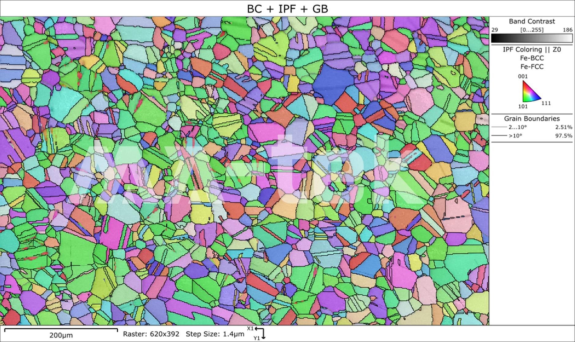
Figure | Orientation Map
Different colors represent different grain orientations. By using EBSD scanning, a grain orientation distribution map of the material can be established, which is used to analyze the microstructure and grain arrangement of the material.
-
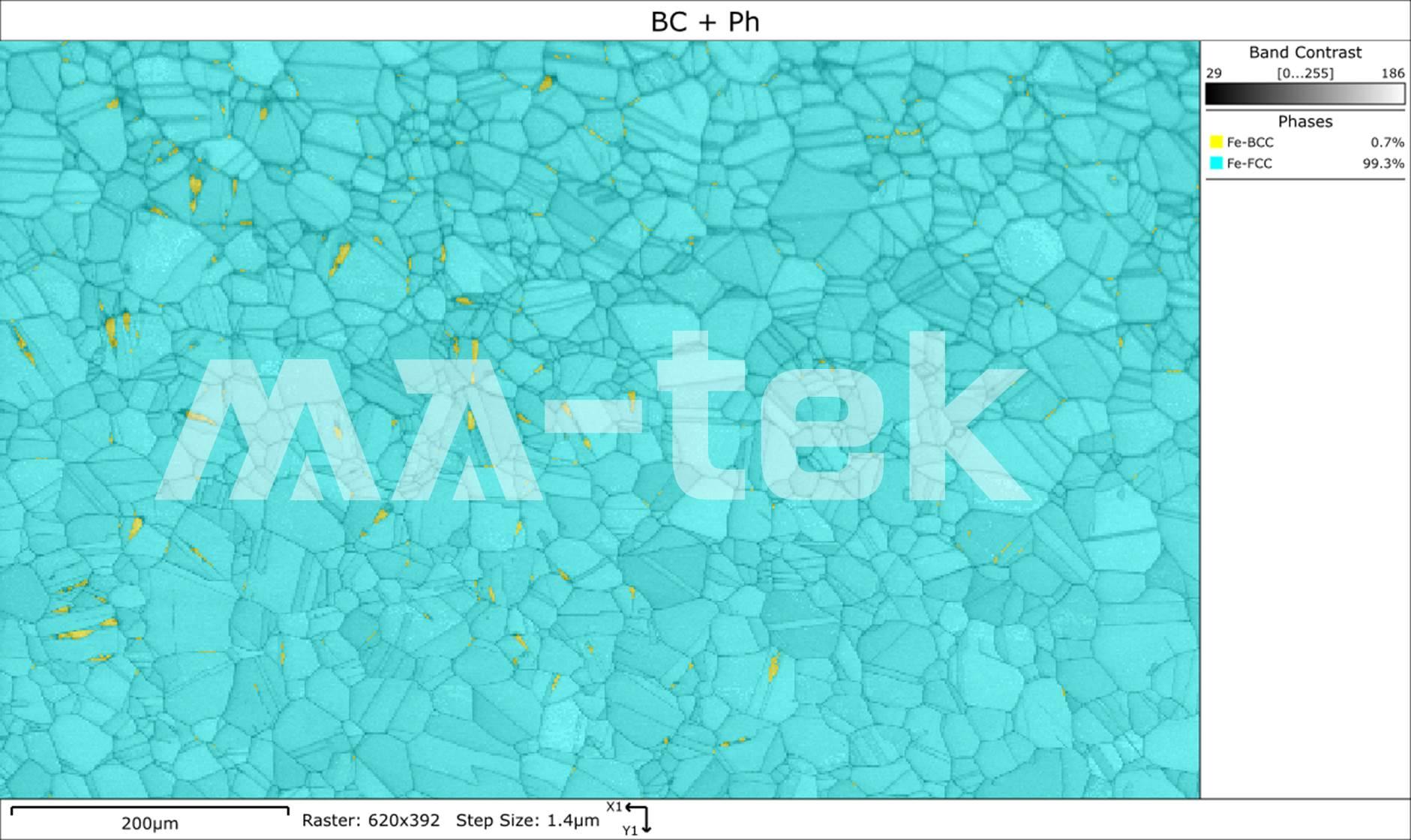
Figure | Phase Map
Different colors represent different crystal phases, which can be used to analyze the phase composition and distribution in materials.
-
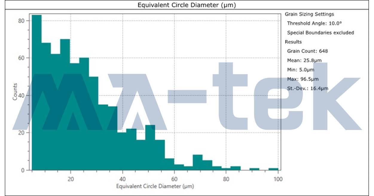
Figure | Grain Size Distribution
Grain size statistical chart, showing the distribution of grain sizes in the material, can be used to assess the impact of material processing and heat treatment on grain growth.
-
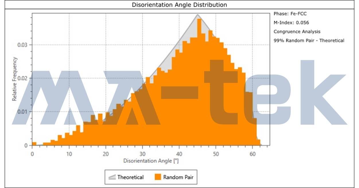
Figure | Misorientation Angle Distribution
The dislocation angle distribution map of grain boundaries can analyze the characteristics of material grain boundaries and the angular relationship between grains.
-
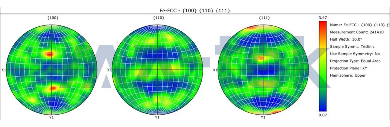
Figure | Pole Figure
Pole figure can be used to analyze the distribution of crystal orientations in materials and assess the texture characteristics of the materials.
-
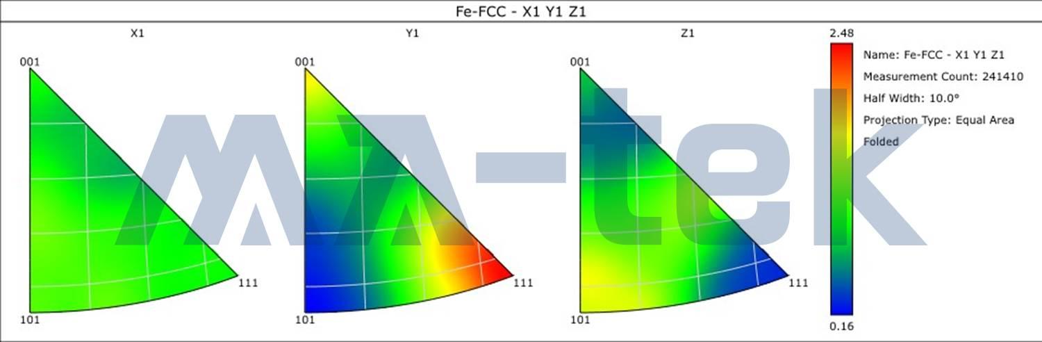
Figure | Inverse Pole Figure
The Inverse Pole Figure (IPF) shows the relationship between grain orientation and the sample coordinate system, and can be used to analyze the crystal orientation distribution of materials.


