
PEM-CCD
PEM-CCD (Photon Emission Microscopy with CCD detector)also known asEMMI (Emission Microscopy)is a widely used inNon-destructive bright spot localization technologyThe principle is to detect due to the operation of the IC.electron-hole recombination or thermal carrier effectsthe weak photons emitted are used to locate abnormal or failure locations within the chip.to assist engineers in determining whether further methods such as InGaAs-PEM, electrical measurements, or destructive analysis are needed to enhance the overall efficiency and success rate of the FA process.
PEM-CCD uses a cooled charge-coupled device (Cooled CCD, C-CCD) as a photon detector, with a detectable wavelength range of approximately400 nm to 1100 nmcovering the visible light and part of the near-infrared region, it has long been a standard tool for initial fault localization in ICs.
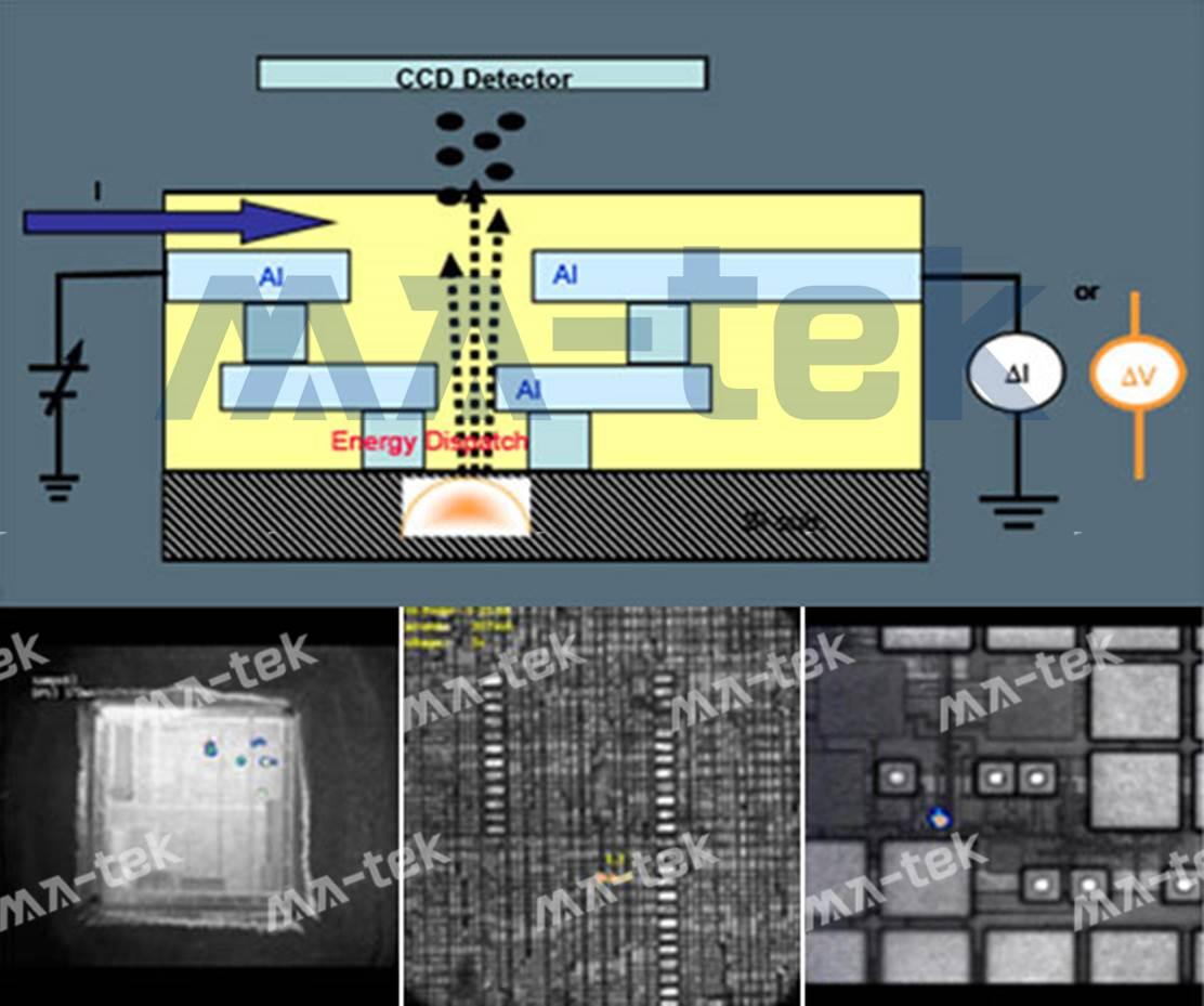
PEM-CCD (EMMI) combines mature photon emission analysis technology with MA-tek's failure analysis expertise to provide a stable, reliable, and efficient solution for IC fault localization. When semiconductor devices experience anomalies, photon emissions may occur due to the following mechanisms:
-
Electron-Hole Recombination
-
Hot Carrier Emission
These photons concentrate in abnormal or failure areas, forming detectable hot spots by PEM-CCD. Through the analysis of the position, distribution, and intensity of the hot spots, engineers can quickly narrow down the failure range, serving as an important basis for subsequent circuit analysis, electrical verification, and physical analysis.
The above figure is a schematic diagram of EMMI photon emission analysis. When the IC is in an abnormal operation or failure state, electron-hole recombination or hot carrier effects release photons, which are collected and imaged by the CCD detector.
The image below is an example of actual analysis results, where the highlighted positions correspond to leakage, short circuit, or abnormal conduction areas within the chip, which can serve as a basis for subsequent circuit analysis and physical analysis.
In practical applications, PEM-CCD is particularly suitable for failure scenarios that produce significant photon emissions.Through hotspot localization, the efficiency of failure analysis can be effectively improved and unnecessary destructive analysis risks can be reduced.
-
P-N junction leakage or breakdown
-
Transistors that malfunction due to open circuits or short circuits
-
Latch-up
-
Gate oxide layer leakage or breakdown
-
Abnormal conduction caused by polysilicon residue
-
Silicon substrate damage
-
Local burn-out components caused by overcurrent
It should be noted that not all EMMI highlights represent actual failures. Photon emissions may also occur under certain normal operating conditions, such as floating gate states, BJTs or MOSFETs operating in saturation, and forward-biased diodes. Therefore, the analysis results of PEM-CCD usually need to be interpreted in conjunction with electrical measurements and circuit behavior to avoid misjudgments.
Since PEM-CCD belongs to photon emission analysis technology, its detection capability may be limited in the following situations, and in such cases, it usually needs to be combined withPEM-InGaAs, OBIRCH, LVP or other advanced FA technologiesConduct cross-analysis.
-
The emission location is obscured by the upper metal or dielectric layer.
-
Deep or embedded junction defects
-
Leakage location under large area metal lines
-
Resistive short circuit or bridging
-
Surface or internal conductive paths in silicon
-
Leakage current is extremely low (below approximately 0.1 µA)
-
Deep experience in failure analysis:Long-term service for advanced processes, automotive, industrial, and high-reliability ICs, capable of quickly determining the properties of bright spots and avoiding misjudgment of false defects.
-
Complete FA technology integration capability:PEM-CCD can seamlessly integrate with InGaAs-PEM, electrical measurements, FIB repair, structural and material analysis, enhancing the success rate of analysis.
-
Professional testing planning and condition setting:Adjust the bias voltage, integration time, and measurement strategy according to the component characteristics, so that weak bright spots can be stably presented.
-
One-Stop Service:From preliminary positioning, in-depth analysis to root cause determination, executed by the same team, shortening the project timeline.


