
3D OM Optical Microscope
3D OM optical microscope uses principles such as optical interference, focal plane stacking, or white light interference to obtain the sample'sstereo height information (Z axis), and simultaneously presents High resolution 2D × 3D structural images,Compared to OM, which can only provide "flat images", 3D OM can display the completesurface profile, roughness, depth difference, defect volume and geometric measurementis an advanced imaging technology of great value in semiconductor, electronic packaging, and materials engineering.
3D OM technology transforms structures that could only be described in two dimensions into three-dimensional models with height information, allowing all process and structural details to be fully quantified, making it an indispensable technology for many engineering analyses.
1. IC Die Size and Packaging Appearance Measurement
3D OM can observe the shape, edge quality, thickness, and cutting consistency of the die with high accuracy, while also measuring issues such as warping, sinking, resin surface fluctuations, and structural tilting of the packaging appearance. This information can be used for cutting process verification, packaging defect assessment, or appearance quality analysis after molding.
-
Die length/width/thickness
-
Edge trimming consistency
-
Chip corner damage
-
RDL thickness and height distribution
-
Bond pad deformation
-
Die attach resin height
2. Solder joints and metal surface 3D structure
3D OM can reconstruct the complete three-dimensional morphology of solder joints, including solder ball diameter, height, volume, wetting angle, and can even present the apparent roughness of the IMC surface and the surface waveform after reflow. 3D OM can simultaneously provide morphology and height, making it particularly suitable for checking the consistency of solder joint appearance and height in PCBA, WLP, Fan-out, and high-density packaging.
-
Solder ball diameter / height
-
Bump / Pillar height difference
-
Wetting behavior
-
Voids external morphology
-
IMC intermetallic compound surface roughness
-
Reflow surface unevenness after
3. Monitoring of packaging and substrate processes
3D OM provides highly repeatable and traceable measurement data on the thickness variation of RDL lines, the flatness of Cu pillar tops, the thickness difference of solder masks, bump coplanarity, and package warpage, making it suitable for advanced packaging processes such as Flip-chip, WLP, Fan-out, and 2.5D/3D IC. This enables process engineers to quickly assess batch differences and process anomalies, which is critical for quality control in mass production.
-
Cu pillar top flatness (Topography)
-
RDL Trace thickness difference
-
Solder mask thickness
-
Bump coplanarity
-
Package warpage
4. Surface analysis of materials and process morphology
3D OM can accurately reveal information such as etching depth, film undulation, micropore shape, crack depth, surface roughness, and more. Due to its non-destructive characteristics, it can be directly applied to the analysis of metals, ceramics, glass, polymers, composite materials, and MEMS microstructures, making it the most efficient three-dimensional measurement method in material science and process development.
-
Roughness Ra / Rq calculation
-
Coating Uniformity Verification
-
Etching depth measurement
-
Differences in film thickness appearance
-
Determination of Micropore Volume
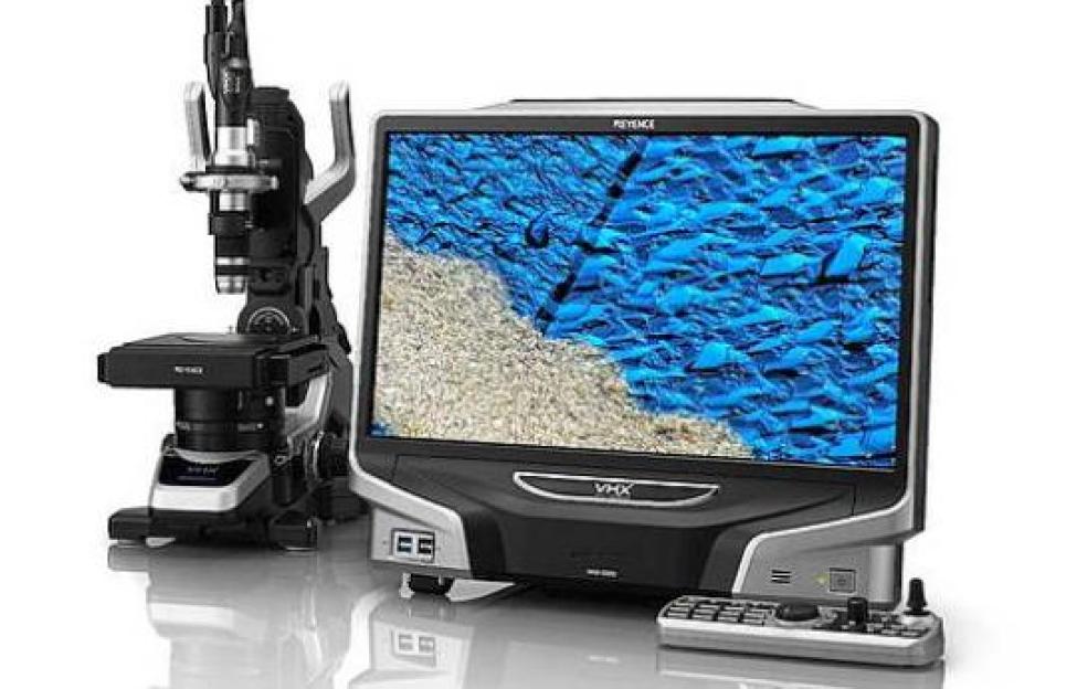
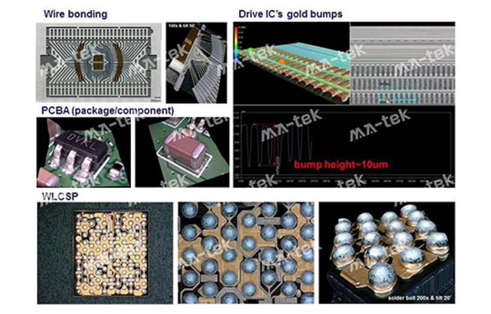
- Three-axis automated 3D imaging:Through Z-axis micro-displacement scanning combined with image algorithms, it can automatically construct a 3D model of the sample, suitable for packaging, precision control processes, MEMS, metal materials, and other fields.
- Real-time 3D Profile and multimodal geometric measurement:3D OM can perform various geometric measurements and has traceability and repeatability, making it a highly useful technology for quality control and process engineering.
- Multi-angle real-time imaging:The 3D OM can capture the observation area from different angles through a variable angle optical path or an inclined sample stage, which is highly advantageous for assessing surface cracks, three-dimensional edges, and stacked structures.
- HDR (High Dynamic Range) high dynamic range imaging:In semiconductor and packaging processes, high-reflective metals (Cu, Al, Au) and low-reflective materials (resin, IMD) often coexist. Traditional OM is prone to overexposure of metals or underexposure of resin, while the HDR technology of 3D OM can simultaneously preserve the details of materials with different reflectivity.
- 50–5000X ultra-wide magnification range:
| Magnification | engineering applications |
|---|---|
| 50–200X | Appearance, packaging defects, wire bonding area observation |
| 200–1000X | solder joint surface, dielectric layer cracks, etching morphology |
| 1000–5000X |
Microfabrication structures, roughness measurement, MEMS features
|


