
Chemical etching to remove encapsulant
Chemical decapsulation is used forsemiconductor device failure analysissample preparation technology, the main purpose of which is to remove the IC packaging.epoxy resinto expose the die and internal gold wire structure for subsequent microscopic analysis, specificchemical acid solution(such as mixed solutions of nitric acid or sulfuric acid), by controlling the temperature, time, and acid concentration, the packaging material is gradually etched and dissolved, andThe structures of the crystal grains, gold wires, and solder pads can be completely preserved.Compared with mechanical decapsulation methods, chemical etching for decapsulation has the following advantages, thus the chemical decapsulation technology is widely used inIC failure analysis, reverse engineering, and packaging quality inspection。
-
Can avoid grain damage caused by mechanical processing.
-
suitable for multi-layer packaging and complex packaging structures
-
can completely preserve the grain and gold wire structure
-
beneficial for subsequent microscopic observation and failure analysis
MA-tek has a completeIC de-packaging and failure analysis technology platformcan choose the most suitable decapsulation method according to different packaging materials and analysis needs. Through the integration of chemical decapsulation and precision microscopic analysis technology, it can effectively expose the die and internal structure, and carry out subsequentOM, SEM, FIB, TEM and other analysis processes,With years of experience in semiconductor material analysis and advanced equipment, MA-tek can provide high-qualityIC failure analysis, packaging structure inspection, and circuit reverse engineering servicesto assist customers in quickly locating problems and improving product reliability.
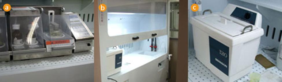
Chemical de-encapsulation equipment
- The automated decapsulation system can control the temperature of the acid solution and the etching time, improving the stability of the decapsulation process.
- Acid bath, used for chemical etching of packaging resin.
- Ultrasonic oscillator, which can accelerate the removal of residues after etching and improve the decapsulation efficiency.
After the chemical delamination is completed, the crystal grains and internal circuit structures will be fully exposed, allowing for further observation and inspection using various microscopic analysis techniques, such as Optical Microscope (OM), Scanning Electron Microscope (SEM), Failure Analysis (FA), and IC Reverse Engineering.
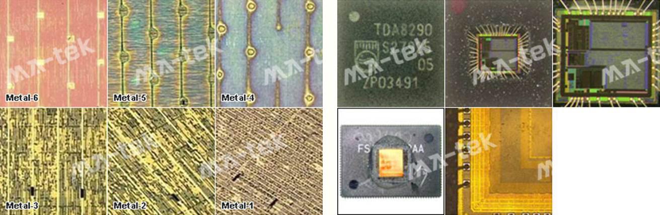
Optical Microscope Observation (OM Imaging)
Using an optical microscope to observe the surface of the die after decapsulation, the interconnection structure of each metal layer in the IC can be identified, and preliminary circuit structure inspection and defect interpretation can be conducted.
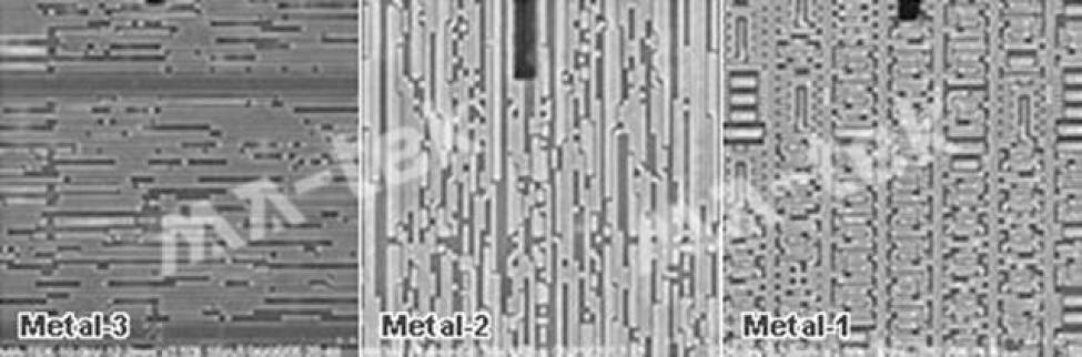
Scanning Electron Microscopy Observation (SEM Imaging)
Using scanning electron microscopy (SEM) allows for further observation of the fine structure of grain surfaces, including metal wires, joints, and circuit layouts, providing high-resolution images to assist in semiconductor failure analysis and reverse engineering.
In failure analysis and reverse engineering, removing the IC packaging resin to expose the die is an important sample preparation step. Currently, common decapsulation methods mainly include chemical etching decapsulation.Chemical Decap) and laser decapsulation (LaserDecapTwo technologies.
Both methods have their applicable situations and technical advantages, chemical etching is suitable forComplete preservation of the grain and gold wire structurethe analysis requirements, while laser decapsulation is suitable forRapid removal of packaging or localized openingthe situation, therefore in the actual failure analysis process, engineers usually rely onPackaging materials, analysis area, and component structureChoose the most suitable de-encapsulation method.
In the actual analysis process, chemical decapsulation and laser decapsulation often willcan be used in combination with each other,e.g., first using Laser De-encapsulationQuickly remove part of the packaging material and reuse it.Chemical etchingFurther removing residual resin, through this integration method, can take into account both.Processing efficiency and grain protectionImprove the success rate of failure analysis and circuit testing.
-
The advantages of chemical de-encapsulation
Complete retention of the chip and internal structure
The biggest advantage of chemical etching for de-encapsulation is that it canUniformly remove packaging materials without easily damaging the chip and gold wire structure.To fully preserve the grain and internal structure, the encapsulation resin can be gradually removed by precisely controlling the temperature, concentration, and etching time of the acid solution, making the grain structure completely exposed, suitable for the following analysis needs:
-
semiconductorFailure Analysis (FA)
-
Bond wireStructural Inspection
-
Observation of Surface Defects on Chips
-
IC circuit reverse engineering
-
-
The advantages of laser de-encapsulation
Fast and precise local de-encapsulation
Laser de-encapsulation uses high-energy laser beams to locally ablate packaging materials, allowing for rapid and precise removal of encapsulation in a short time, suitable forSituations that require quick decapsulation or localized observation。
-
Processing speed is fast
-
Can accurately control the opening area.
-
suitable for local structural observation
However, during the laser processing, thermal effects can occur, and if not properly controlled, it may cause damage to the die or gold wire. Therefore, in high-precision analysis, it is still necessary to combine other decapsulation methods.
-
| technology | Chemical De-encapsulation | Laser de-encapsulation |
|---|---|---|
| Principle | Dissolving packaging resin using acidic solution | Using laser energy to ablate packaging materials |
| Processing method | Chemical etching | Laser thermal processing |
| Removal range | Large area package removal | Local precision delamination |
| Process time | Longer | Faster |
| Process time | low risk | Need to control thermal effects |
| suitable for application | Failure analysis, circuit observation | Partial opening, rapid analysis |


