3D X-ray
3D X-ray (High Resolution 3D X-ray Microscope) captures multi-angle images through sample rotation,and use computer reconstruction of three-dimensional structures, allowing engineers to observe internal defects from different angles and even perform virtual slice analysis. This enhances the interpretative capability of 3D X-ray in the analysis of complex packaging structures, TSV, MEMS components, and multilayer PCBs.
Since the X-ray inspection process does not damage the sample, therefore3D X-ray is an important non-destructive testing tool for failure analysis in IC packaging, MEMS components, and electronic modules.
3D X-ray technology primarily obtains three-dimensional images through the following process:
-
Sample rotation scanning:The X-ray source irradiates the sample while the sample rotates 360°.
-
Multi-angle imaging acquisition:Acquire a large number of X-ray projection images from different angles.
-
Computer reconstruction algorithm:Through CT reconstruction algorithms, image stacking generates three-dimensional volume images (3D Volume).
-
Three-dimensional structural analysis:Virtual Cross Section analysis can be performed in any direction, allowing observation of the internal structures and defects of the sample.
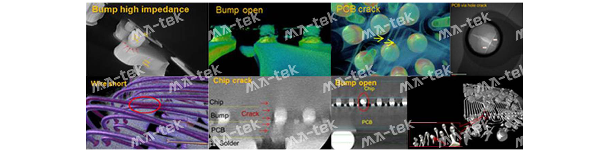
This technology allows for clear identification of internal structures in packaging, such as: solder voids, wire fractures, wire bonding deformations, TSV structural defects, internal cracks in PCBs, etc.
-
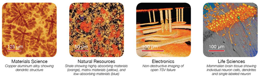
Microelectronics and Semiconductors
-
IC packaging internal structure inspection
-
BGA / Flip-chip solder defect analysis
-
TSV structural defect detection
-
Observation of internal structures of MEMS components
-
-
Electronics and Circuit Boards
-
Internal wire structure analysis of PCB
-
Solder void ratio detection
-
Soldering defects and crack detection
-
-
Materials Science
-
Analysis of internal structures in materials
-
Observation of Hole and Crack Distribution
-
-
life sciences
Observation of three-dimensional structures of biological samples
In the inspection of electronic components and semiconductor packaging, both 2D X-ray and 3D X-ray are common non-destructive testing techniques. Both utilize the contrast of images after X-rays penetrate materials to observe internal structures, but there are still significant differences in the way images are presented and the analytical capabilities.
2D X-rayMainly through X-ray penetrating the sample in a single direction to form a flat image, thus the image will contain all structural information along the ray path. This method is suitable for quickly inspecting solder joints, wire bonding, and packaging structures, such as BGA solder ball voids and wire bond morphology.
In contrast, 3D X-rayThe technology captures multi-angle X-ray images by rotating the sample and then uses computer calculations to reconstruct the three-dimensional structure. This method clearly presents the internal structures and defect locations of the sample and provides complete three-dimensional information. Therefore, in practical analysis processes, it is common to first use2D X-ray conducts quick screening, then use 3D X-ray conducts in-depth structural analysis and defect localization.。
| Comparison items | 2D X-ray | 3D X-ray |
|---|---|---|
| Image format | two-dimensional projection image | three-dimensional structure |
| Scanning method | Single Angle Penetration | Multi-angle rotation scanning |
| Image Information | Multi-layer structures may overlap. | Layered observation of internal structures |
| Analytical ability | suitable for quick checks | suitable for precise defect localization |
| Common Applications | PCB solder joints, wire bonding observation | TSV, MEMS, 3D IC, packaging defects |
-
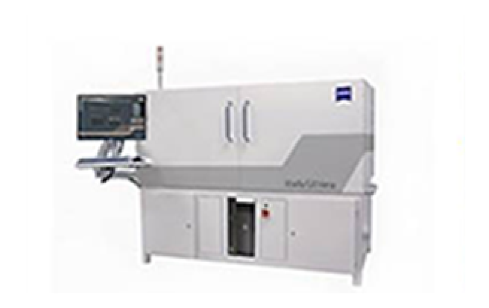
Image | High-Resolution 3D X-ray Equipment
-
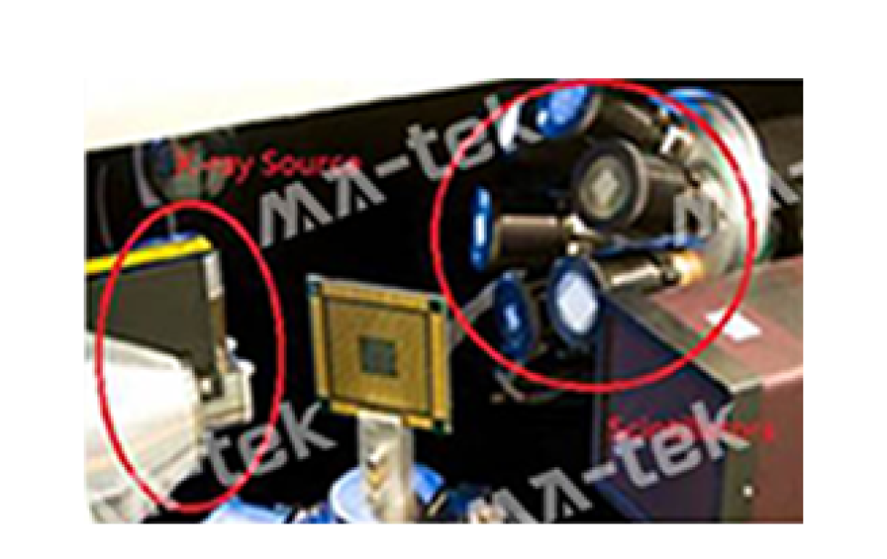
Figure | 3D X-ray light source and detection system configuration, which can obtain multi-angle images by rotating the sample.
MA-tekWith years of experience in semiconductor material analysis and failure analysis, a complete packaging structure inspection platform has been established. Through high-resolution 3D X-ray systems and cross-technology integration capabilities, more accurate defect localization and structural analysis can be provided to customers.
- High-resolution three-dimensional structural analysis:It can obtain three-dimensional images at the nano to micro scale, clearly presenting the internal structure of the package, solder joint morphology, and material interfaces.
- Non-destructive defect localization:Non-destructive observation of internal defects in the package can be performed, such as solder voids, TSV defects, cracks, or wire breaks.
- Cross-technology integration analysis capability:Can be integrated with various failure analysis techniques, through multi-technology integration, a complete analysis process can be formed:Non-destructive testing → Defect localization → Cross-section verification → Root cause analysis
- Support for various advanced packaging technologies:2.5D / 3D IC, TSV structure, MEMS components, Flip-chip / BGA packaging, high-density PCB, etc.
-
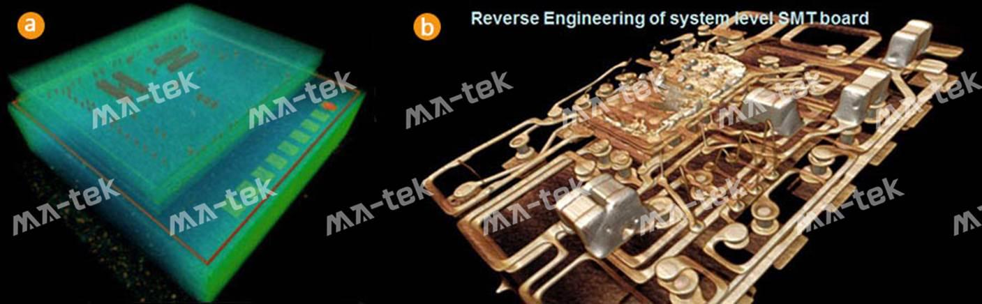
Figure | IC Packaging and System Module Analysis
(a) 3D structural images of MEMS IC; (b) SMT system circuit board reverse engineering
3D X-ray can completely reconstruct the internal structure of electronic modules, assisting engineers in analyzing packaging and circuit layout.
-
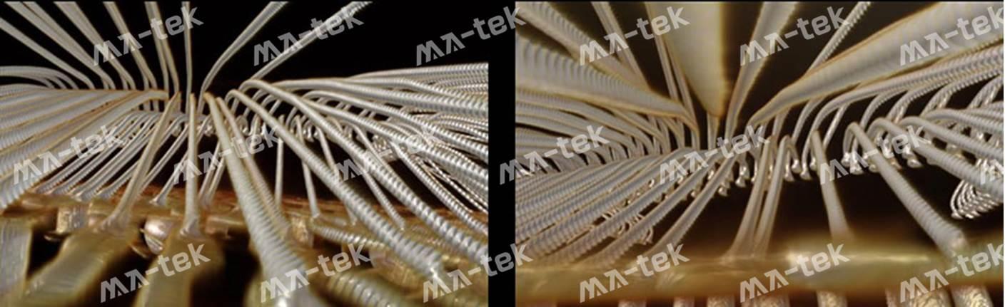
Figure | Analysis of Packaging Wire Bond Structure - Copper Wire (Cu Wire) Wire Bond Structure
Through 3D X-ray, the morphology and arrangement of the internal copper wire bonding in the package can be clearly observed, including the bonding height, morphology, and potential lifting or fracture issues.
-
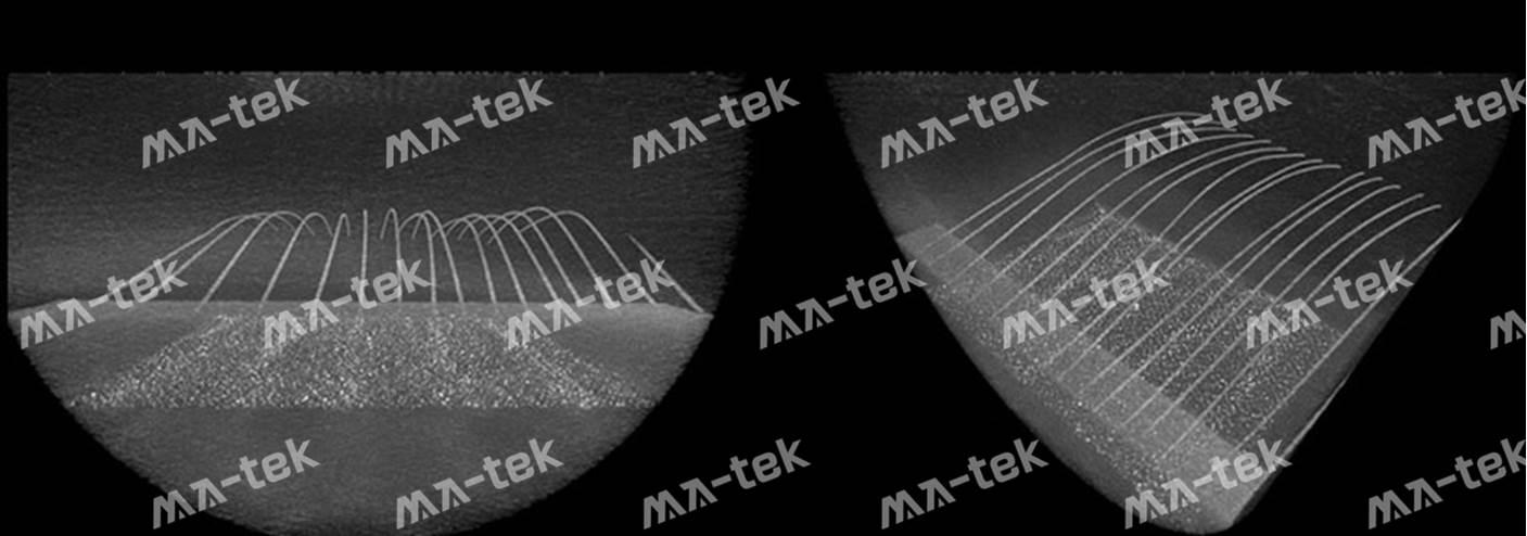
Figure | Package Wire Bond Structure Analysis - Aluminum Wire Bonding (Al Wire Bonding)
The structure and connection status of aluminum wire bonding in X-ray images.
-
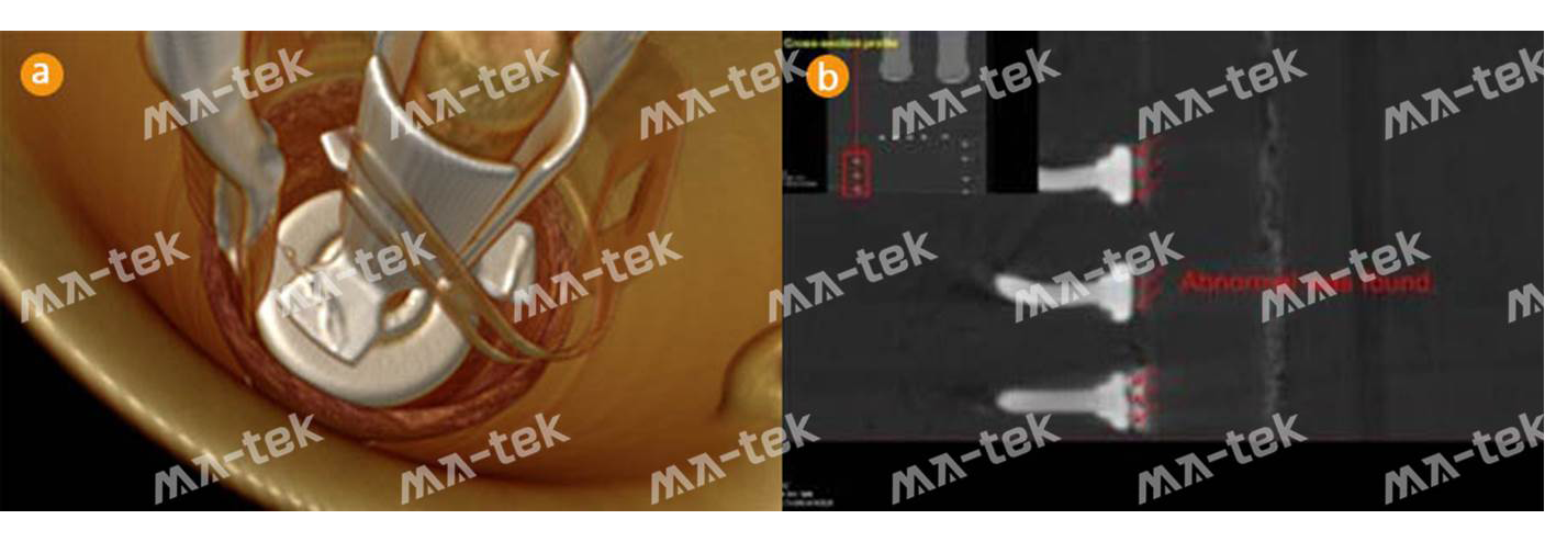
Figure | Mechanical components and packaging defects
(a) Micro motor structure; (b) Wire lifting defect
Can analyze internal defects in structures and electronic components.
-
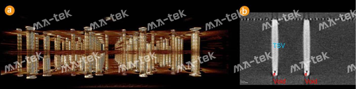
Figure | PCB and TSV Structure Analysis
(a) PCB substrate; (b) TSV void defect
3D X-ray can clearly observe voids or filling defects in the TSV structure.
-
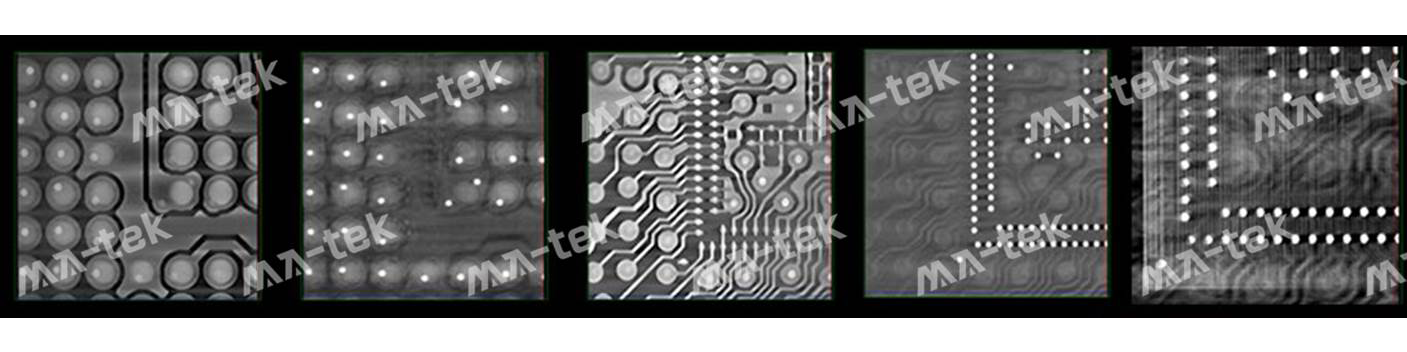
Image | PCB Circuit Layout 3D X-ray Image
Images of internal wiring and circuit layout of the PCB.