
SEM scanning electron microscope
Scanning Electron Microscope (SEM), also known as scanning electron microscope,is a high-resolution microscopic analysis technique that uses a high-energy electron beam to scan the surface of a sample and forms images based on signals generated by the interaction between electrons and the material.Compared to traditional optical microscopes, SEM can provide higher resolution and depth of field, allowing researchers to clearly observe the surface morphology and structural features of materials at the nanoscale to microscale.
In the SEM operation process, the electron gun generates a high-energy electron beam, which is focused by electromagnetic lenses to scan the surface of the sample. When the electron beam interacts with the atoms of the sample, various signals are produced, including secondary electrons (SE), backscattered electrons (BSE), and characteristic X-rays. By collecting and converting these signals through different detectors, high-resolution and high-contrast images can be established for observing the surface morphology, structural features, and material differences of the sample.
To further enhance the capability of material composition analysis, SEM is usually paired with Energy Dispersive Spectroscopy (EDS), which can perform elemental analysis on micro-regions, providing qualitative and semi-quantitative information about material composition. It can also conduct point analysis, line scanning, and elemental mapping, assisting in the determination of material composition, foreign material sources, and contaminant components. Energy Dispersive Spectroscopy is also known as Energy-dispersive X-ray spectroscopy, with English abbreviations including EDS, EDX, EDXS, or XEDS.
In the analysis of semiconductor devices and electronic materials, SEM is often combined with various sample preparation techniques, such as Ion Milling, Focused Ion Beam (FIB) cross-section preparation, and Delayer techniques, allowing analysts to observe the internal multilayer structures of chips, metal interconnections, dielectric layers, and contact interfaces, as well as to perform precise size measurements and defect determinations.
- Microstructure observation:SEM can perform high-resolution surface and cross-sectional observations of various materials and electronic components, analyzing structural features at the nano to micro scale, such as metal interconnects, dielectric layer structures, and fine patterns.
- Film and structure size measurement:Cross-sectional observation of multilayer structure samples allows for precise measurement of film thickness, line width, and structural dimensions, as well as assessment of process quality and structural integrity.
- Elemental analysis (EDS):Through X-ray spectral analysis for element identification and semi-quantitative analysis, it is possible to determine material composition, sources of foreign substances, and the composition of contaminants.
- Electrical defect observation (PVC):Using low acceleration voltage electron beam scanning for Passive Voltage Contrast (PVC) analysis can detect open circuits, leakage, or high resistance abnormal locations.
- IC reverse engineering and circuit restoration:Combined with Delayer layer removal technology and automatic image stitching, a complete circuit structure image can be established, providing important information for integrated circuit reverse engineering and circuit analysis.
- Failure analysis integrated applications:SEM can be integrated with various failure analysis techniques, such as EMMI (Emission Microscopy), OBIRCH (Optical Beam Induced Resistance Change), Nano-probing, FIB cross-section analysis, etc. Through cross-technology integration, it can significantly improve defect localization efficiency and accurately analyze component failure mechanisms.
MA-tek has accumulated many years of practical experience in the field of semiconductor and electronic component analysis, establishing a complete SEM analysis platform. Through the integration of high-resolution SEM equipment and comprehensive analysis techniques, MA-tek is able to assist customers in quickly locating defects, analyzing microstructure issues, and providing highly reliable material and component analysis results.
- High-resolution FE-SEM equipment:Multiple field emission scanning electron microscopes are configured for nanoscale microstructure observation.
- Complete sample preparation technology:Combining FIB, Ion Milling, and Delayer preparation techniques, providing high-quality cross-sectional observation and structural analysis.
- Cross-technology failure analysis platform:SEM can be integrated with EMMI, OBIRCH, Nano-probing, SAT, and X-ray technologies to establish a complete fault localization and analysis process.
- Professional Analysis Team:With rich experience in semiconductor processes and component analysis, capable of quickly interpreting images and providing precise failure mechanism analysis.
MA-tek has established multiple high-resolution Field Emission Scanning Electron Microscopes (FE-SEM), which can provide nanoscale structural observation and material analysis capabilities. The field emission electron gun has high brightness and low energy spread characteristics, allowing it to maintain high-resolution imaging capabilities under low acceleration voltage conditions, making it particularly suitable for advanced process nodes and nanoscale microstructure observation.
-
Hitachi S-4800 FE-SEM
-
Hitachi S-8020 FE-SEM
-
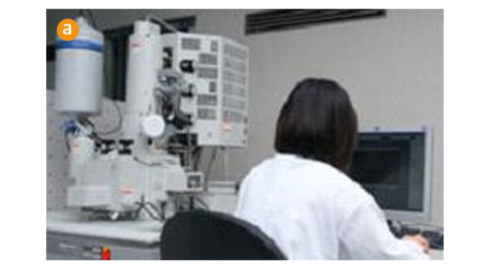
Image | Hitachi S-4800 FE-SEM
-
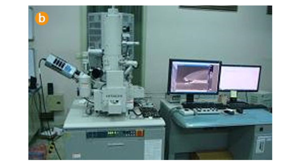
Image | Hitachi SU-8220 Field Emission Scanning Electron Microscope Equipment
-
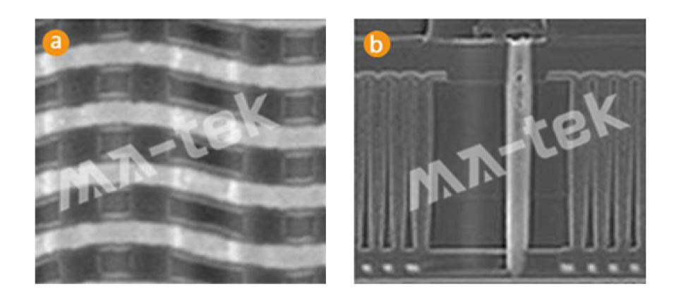
(a) Dynamic Random Access Memory (DRAM) cell planar structure observed from the top view of SEM after the removal of capacitor materials can be used to analyze cell structure and process morphology.
(b) Cross-sectional SEM image of the DRAM word line contact, used to observe the contact structure and the quality of the multi-layer interconnection process.
-
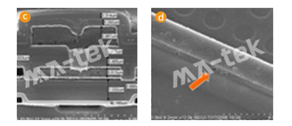
(c) Cross-sectional analysis of multi-layer metal and dielectric structures in DRAM can assess the structural integrity of the components and process variations.
(d) Planar SEM top view observation shows the localized damage locations of the component after electrostatic discharge (ESD) testing, used for failure analysis and defect localization.
-
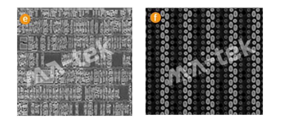
(e) Integrated circuit metal line structure images can be applied to circuit restoration and reverse engineering analysis.
(f) Passive Voltage Contrast (PVC) images can identify areas of electrical anomalies and the locations of open defects.
-


