
OM Optical Microscope
Optical microscope utilizationVisible light (wavelength 400–700 nm)When irradiating, different image contrasts are formed when light interacts with the sample surface to produce reflection or scattering. However, since the wavelength of visible light is longer, the theoretical resolution of OM (i.e., the minimum distance at which two points can be resolved) is only about0.2 μmThis also makes OM'sThe maximum effective magnification is about 1000X.The function of OM is not to "analyze nanometer details," but to "quickly obtain a complete macro structural status," which is the starting point for all in-depth analysis.
- Although the resolution is not as good as that of electron microscopes (SEM/TEM), OM has significant advantages:
- Large field of view: can quickly scan large areas, making it the best tool for assessing process consistency and identifying widespread defects.
- High speed: suitable for mass production monitoring, process comparison, and failure localization.
- High tolerance: suitable for various samples such as metal layers, silicon wafers, packaging bodies, PCBs, cross-sections, Delayer, etc.
- Non-destructive: No vacuum or metal coating is required, allowing for rapid observation in the original state of the sample.
Optical microscopes (OM) cannot resolve details at the nanoscale, but theirHigh field of view, high speed, low destructiveness, and high toleranceThe characteristics make it the most commonly used and the most valuable observation method in real-time in the fields of electronics, semiconductors, and materials. The following are the most representative analytical uses and engineering scenarios of OM in the industry:
1. Cross-section Analysis
After cross-section preparation, the overall structural arrangement and interface behavior of the sample can be clearly observed through OM, making it the most commonly used preliminary structural inspection method in packaging, PCB, module, and materials engineering.
| Observable content | Application scenarios |
|---|---|
|
|
2. IC Delayer structure confirmation
Delayer analysis (planar delayering) involves the stepwise removal of metal and dielectric layers to observe the internal circuit structure without damaging the operational logic of the chip. OM is the most important preliminary observation and process monitoring tool in IC delayering analysis.
| Observable content | Application Scenarios |
|---|---|
|
|
3. Precipitate Free Zone (PFZ) analysis
PFZ is a zone of depletion of precipitates that appears near the grain boundaries in metallic materials (such as aluminum alloys) after heat treatment or strain. It is an important parameter in materials engineering used to assess the effects of heat treatment and material degradation.
| Observable content | Application scenarios |
|---|---|
|
|
4. Dislocation lines, etching anomalies, and crystal defects observation
OM can quickly identify surface defects caused by crystal growth, heat treatment, or etching processes, making it an important inspection item in the front-end-of-line (FEOL) processes and materials research.
| Observable content | Application scenarios |
|---|---|
|
|
5. Oxidation stacking faults(Oxidation Induce Stacking Fault, OISF) Study
Oxidation stacking faults are stacking faults generated during high-temperature oxidation processes due to the diffusion of twin defects or crystal defects. OM can clearly present the distribution and diffusion profile of oxidation stacking faults, which is an important quality indicator for silicon wafer materials, used in growth and oxidation process analysis.
| Observable content | Application Scenarios |
|---|---|
|
|
MA-tek offers a variety of OM optical microscopes, covering a complete imaging capability from low magnification wide-field observation to high magnification fine structure identification, allowing for in-depth presentation of material structures, surface morphology, and process characteristics, meeting the observation needs of different fields such as semiconductors, packaging, and materials engineering.
-
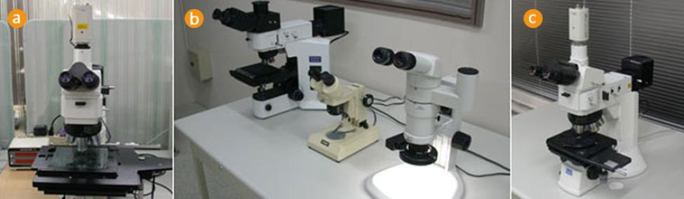
Figure | (a) 50-1000X (b) 100-500X / 40-200X / 5-75X (c) 50-1000X
-
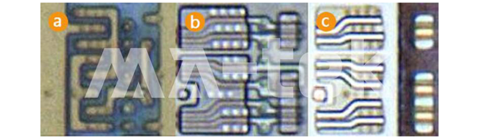
Figure | (a) Metal (b) Poly (c) OD/AA
| magnification | Magnification range | Application |
|---|---|---|
| 50–1000X | High magnification, used for IC delayering, metal layer structure, interface observation, and detection of small defects (such as over-etch, IMD anomalies, etc.). | High-resolution structural comparison, micro defect and process anomaly localization, Delayer fine layer analysis |
| 100–500X | Medium to high magnification is used for PCB/PCBA solder joints, packaging interfaces, film thickness, and metal distribution analysis. | solder joint IMC, packaging interface, metal layer and wire morphology |
| 40–200X | Medium magnification is used for grain analysis, delayer layer position confirmation, and preliminary structural inspection. | Structural layer confirmation, grain analysis, etching profile scanning |
| 5–75X | Low magnification with a wide field of view is used for appearance inspection, cross-section scanning, wafer breakage, packaging delamination, and other macro defect localization. | Appearance inspection, cross-section large field of view, packaging failure, wafer defect scanning |


