Chat with us, powered by LiveChat

AFM Atomic Force Microscope

Technical Principles

Atomic Force Microscope (AFMis a high-resolution scanning probe microscopy technique used to measure the surface of materials.Nano-scale morphology and structural featuresAFM scans the surface of the sample using a nanoscale probe, utilizing the atomic interactions between the probe and the sample to create a slight deflection of the probe cantilever. Laser light is directed onto the back of the cantilever and reflected to a light detector, where the amount of deflection of the reflected light can be converted into height information of the sample surface, thereby establishingHigh-resolution surface morphology images,Therefore, it is widely used in the research of semiconductor materials and nanomaterials.


In the early days, AFM mostly used Contact Mode.Conduct measurements, and currently commonly usedTapping Mode can effectively reduce the scratching and contamination effects caused by the contact between the probe and the sample, enhancing measurement stability. In addition, AFM can also be combined with different modules for various physical property measurements, such as:Electrical analysis,Magnetic analysis,Doping Distribution Analysis (SCM Module)
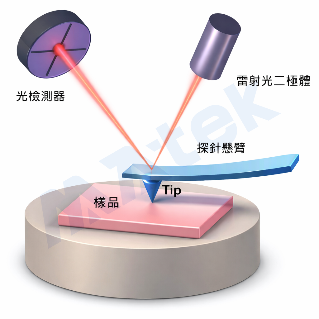


AFM measurement principle diagram

AFM uses a nanoscale probe (Tip) to scan the surface of the sample. When atomic interactions (such as van der Waals forces) occur between the probe and the sample, it causes a slight displacement of the probe's cantilever (Cantilever).

The laser light is directed onto the back of the cantilever and reflected to the light detector. When the cantilever is deflected due to surface forces, the position of the reflected light also changes. By detecting the laser deflection and converting it into a signal, the surface morphology and nanoscale structure of the sample can be reconstructed.
 
Analysis Application
Semiconductor Material Analysis
The maximum sample size supports measurement and analysis of 12-inch wafers.
Film and Structural Defect Analysis
Can scan to observe thin film coatings, microstructures, and surface defects.
Three-dimensional surface image analysis
Create a 3D morphological image of the material surface.
Micro area size and height measurement
Measuring the size and height differences of small structures.
Surface Roughness Analysis
Analyze the nanoscale roughness (Roughness) of the material surface.
Surface morphology measurement
High-resolution surface morphology that can be measured in the range of 100 μm or less.
Types of machines

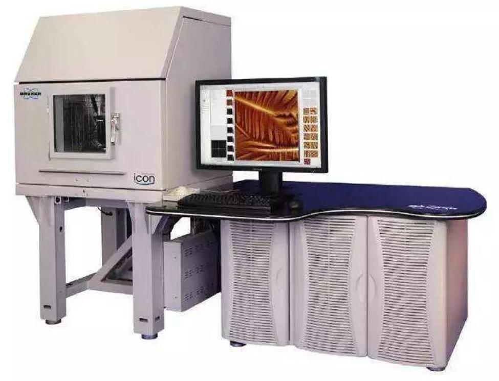
AFM ( Bruker ICON )

It can perform high-resolution surface morphology and property analysis at the nanoscale. Dimension Icon is a research-grade AFM platform, equipped with a highly stable scanning system and various measurement modes, providing precise information on nanoscale structures and surface characteristics.The system can performNanoscale three-dimensional surface morphology measurementand can be equipped with various functional modules for electrical, mechanical, and material property analysis, making it widely applicable in semiconductor, nanomaterials, and advanced packaging research.


System Features

  • Nanoscale surface morphology measurement capability

  • High stability scanning platform and low noise design

  • Supports multiple measurement modes (Contact / Tapping / PeakForce, etc.)

  • Can be equipped with various functional modules for property measurement.

  • Applicable to semiconductor and nanomaterials analysis

Application examples
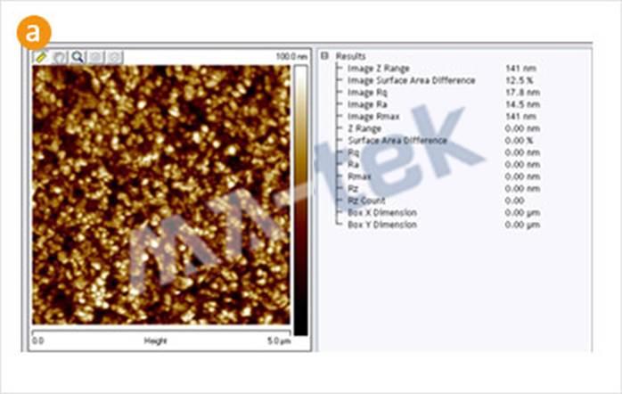
  • (a) Surface Roughness Analysis

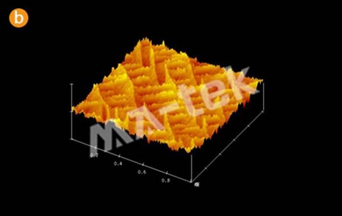
  • (b) 3D imaging

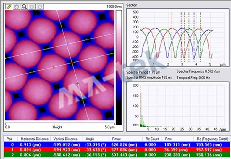
  • Section analysis

Contact
Contact Window
Taiwan Laboratory

Mr. Liu

Ext. +886-3-6116678 ext:3972
Shanghai Laboratory

Mr. Yang

Ext. +86-21-5079-3616 ext:7201

Privacy Preference Center

We use cookies to allow our website to function properly, personalize content and advertisements, provide social media features, and analyze traffic. We also share information about your usage of our website with social media, advertising, and analytics partners.

View Privacy Policy

Manage Consent Settings

Necessary Cookies

Always Enabled

The operation of the website relies on these cookies, and you cannot disable them in the system. These cookies are usually set based on the actions you take (i.e., service requests), such as setting privacy preferences, logging in, or filling out forms. You can configure your browser to block or prompt you about these cookies, but this may result in certain website functionalities not working.