
Solar cells are composed of multiple layers of thin films and functional structures, including an anti-reflective coating (ARC), emitter, metal electrodes, and back surface aluminum layer (BSF). The thickness and material quality of each layer directly affect light absorption efficiency, carrier transport capability, and overall conversion efficiency. Through thin film and layer structure analysis, a complete understanding of the solar cell's cross-sectional structure, material composition, and interface quality can be achieved, assisting in process optimization and enhancing cell performance and reliability.
Key Points of Solar Cell Thin Film Structure Analysis
Conduct cross-sectional observation and material identification of the multilayer film stacking structure of solar cells to confirm whether each functional layer meets the process design requirements.
Common analysis items include:
- Measurement of anti-reflection layer thickness
- Thin film thickness analysis
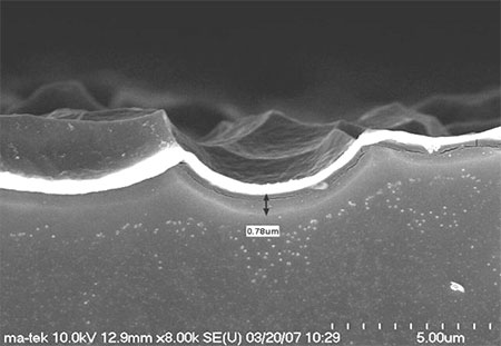
- Analysis of the emitter layer structure
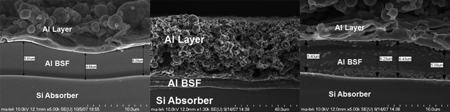
- Backside aluminum BSF structure analysis
- Observation of multilayer film stacking structure
- Thin film material composition analysis
Commonly Used Techniques
- SEM / EDS
- TEM
- FIB cross-section analysis
SEM - BSF staining
SEM - Emission Tip Junction Staining
substrate pinhole
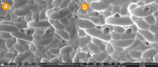
(a) FIB image; (b) SEM image
FIB cutting substrate pinhole
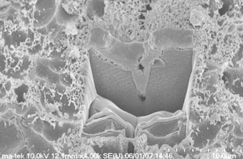
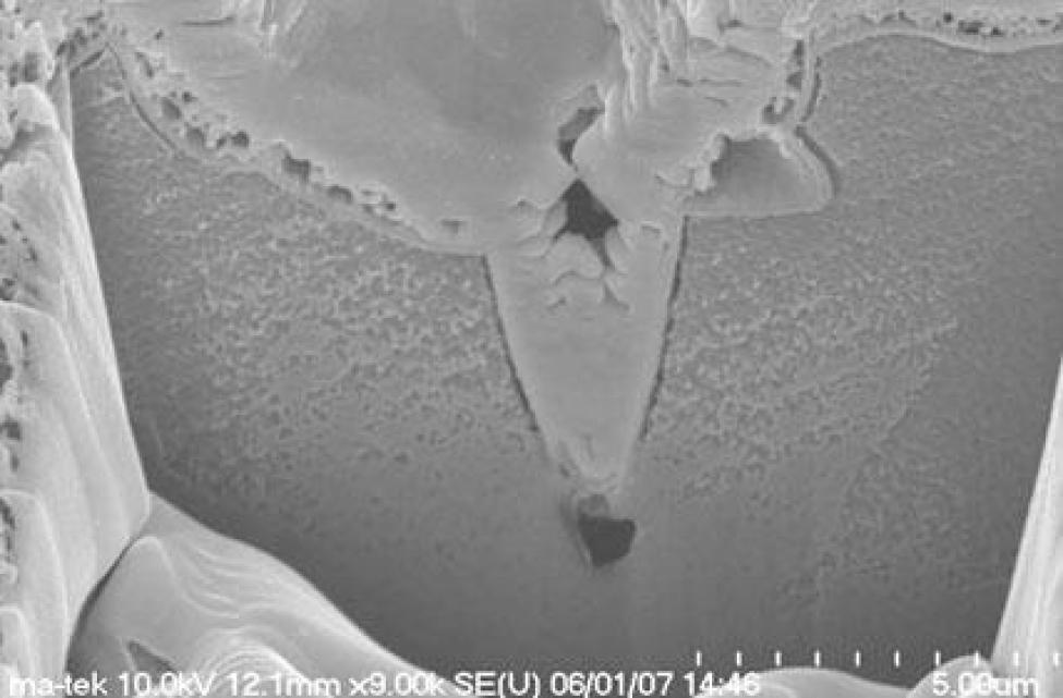
substrate pinhole(X-TEM)
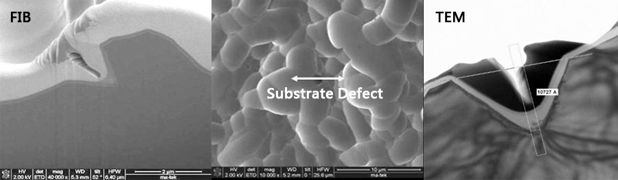
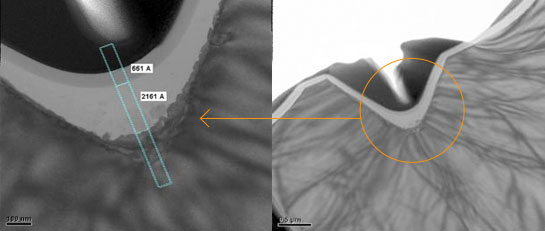
cross-sectionTEM


