
Variable Measurement
Strain measurement is to convertMechanical deformation is converted into quantifiable engineering data.the key technology used forObjective quantification of the mechanical deformation degree endured by circuit boards (PCB/PWB) during assembly, testing, and actual operation.It can directly reflect the impact of PCB structural deformation on the reliability of SMT solder joints, widely used inboard-level reliabilityUnder evaluation.
In mechanical engineering, structures undergo shape changes under external forces, which may arise from tension, compression, shear, bending, or torsion. For electronic products, the bending or warping of PCBs transmits mechanical stress to SMT components and solder joints, potentially leading to cracks, fatigue, or electrical failure.
The purpose of strain measurement is to convert this type ofInvisible micro-deformations are converted into quantifiable engineering data.As the basis for solder joint reliability analysis and design risk assessment, MA-tek adheres to IPC international standards, combining precise strain measurement and electrical monitoring technology to assist clients in managing risks in real-time and enhancing overall board-level reliability during product design, manufacturing, and reliability validation stages.
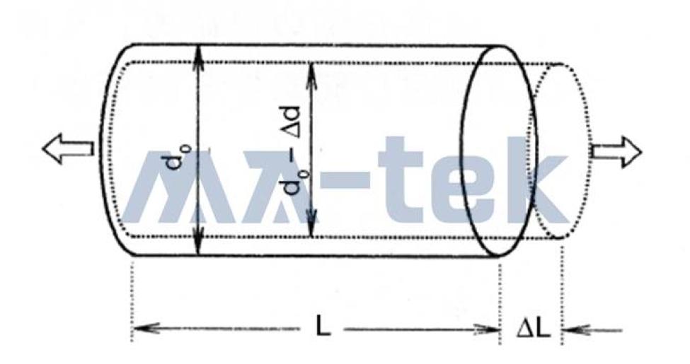
Strain (ε) is used to describe the deformation produced in a structure under the action of external forces.relative deformation degreethe elongation (or compression) of the structure after being subjected to force, relative to the original length. Since strain is the "deformation ratio per unit length," it is thereforeStrain itself is a dimensionless ratio.often expressed in microstrain (με, microstrain).
Strain formula | Quantitative representation of structural deformation
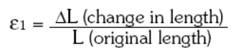
-
ΔLThe change in length of a structure after being subjected to force.
-
Lthe original length of the structure
- The formula can be used to describe tensile strain and compressive strain, and serves as the basic calculation method for plate-level bending and weld point stress analysis.
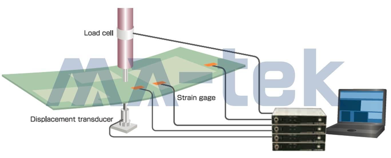
In actual board-level reliability testing, strain measurement is usually conducted throughStrain GaugeAttached to specific locations on the PCB surface to measure the real-time strain changes of the circuit board under external forces or bending loads,Measurement systems typically include:
-
Strain Gauge: Sensing small deformations on the PCB surface
-
Displacement Sensor: Measure board bending displacement
-
Load Cell: Measures the magnitude of the applied external force.
-
Data Acquisition System (DAQ): Synchronously recording changes in strain, displacement, and force.
Through these measurement data, a foundation can be establishedThe correspondence between PCB bending amount, strain distribution, and the stress on solder joints.。
-
Measurement Purpose | Establishing the Correlation Between PCB Deformation and Solder Joint Failure
The core purpose of strain measurement is to:
-
Quantify the strain levels experienced by SMT components during the PCB assembly, testing, and operation processes.
-
Assessing the stress state and risk of solder joints under different board bending conditions.
-
Establish critical strain thresholds for PCB deformation and solder joint failure.
-
As a key auxiliary measurement for board-level drop, bending, thermal cycling, and other reliability tests.
Through strain data, a traceable and comparable engineering model can be established between "structural deformation" and "solder joint reliability."
-
-
Specification Basis and Failure Assessment | IPC-9704 Strain Measurement Standards
Strain measurement is generally performed according to IPC-9704 standards, which define:
-
Strain gauge bonding position and direction
-
Measurement methods and calibration methods
-
Criteria for Strain Data Acquisition and Analysis
In board-level reliability applications, strain measurement is often conducted in conjunction with real-time resistance monitoring of solder joints. When a 20% increase in the resistance value of the solder joint compared to the initial value is detected during the testing process, it can be determined that the solder joint has failed, and the strain level of the PCB at that moment can be traced back as a basis for judging the critical condition of failure.
-
Strain measurement has high practical value in the electronics industry and is often applied to:
-
SMT packaging and solder joint reliability risk assessment
-
Auxiliary measurements for board-level drop, bending, and cyclic bending tests
-
Optimization of PCB structural design and thickness selection
-
Analysis of the impact of process operations (such as pressing and locking) on solder joint.
-
Establishing Design Strain Limit
Through strain measurement, potential solder joint failure risks can be grasped in advance before product design and mass production.


