
FIB Focused Ion Beam Microscope
Focused Ion Beam (FIB) is a precision analysis technique that utilizes high-energy ion beams for nanoscale processing, cross-section preparation, and microstructure analysis of materials. By focusing high-energy ion beams on the surface of the sample, precise sputtering, etching, and deposition of materials can be performed, thus FIB is also commonly referred to asNano-scale processing tools or nano carving knives。
In the fields of semiconductor process development, failure analysis, and materials research, FIB can perform nanoscale precise cutting and sample preparation at specific locations, and can be combined with scanning electron microscopy (SEM) to formDual Beam FIB-SEMIt possesses high-resolution imaging observation and micro-area processing capabilities, making it an indispensable core equipment for advanced semiconductor analysis.
The Focused Ion Beam microscope primarily uses a Gallium (Ga) Liquid Metal Ion Source (LMIS)As an ion beam source. The melting point of gallium metal is about 29.76°C, and under vacuum conditions, a stable liquid metal ion source can be formed. When liquid gallium flows along the metal tip and a high electric field is applied, the tip will form aTaylor coneAt this time, gallium atoms are ionized and ejected to form a high-energy ion beam. After being focused by the electromagnetic lens system, it can form a diameter of less than10 nmThe high-energy ion beam, due to its high kinetic energy and high current density (about 10⁶ A/cm²·sr), can perform precise sputtering and processing on the material surface, achieving nanoscale cutting and material removal.
The FIB system includes a liquid metal ion source (LMIS), a focusing and scanning lens system, a precision sample movement platform, a gas injection system (GIS), and electronic or ion signal detectors. In advanced analytical equipment, FIB is usually combined with SEM to formDual Beam FIB-SEMThrough the combination of electron beam observation and ion beam processing, high-precision processing and analysis can be completed without damaging the surrounding structures.
-
Electron Beam (SEM)Used for high-resolution imaging observation and positioning.
-
FIBUsed for precise nanoscale cutting, material deposition, and TEM sample preparation.
- Circuit Editing: Circuit repair, wire cutting, and reconnection can be performed through ion beam etching and metal deposition techniques to quickly verify chip designs.
- Cross-section Analysis: It allows precise cutting of samples at specific locations and observing microstructures through SEM, used for process defect analysis and structural confirmation.
- Ion Channeling Contrast: Utilizing the interaction between crystal structure and ion beam to observe differences in grain orientation and crystal structure.
- TEM sample preparation: ultra-thin samples at the nanoscale can be prepared for high-resolution analysis using transmission electron microscopy (TEM).
MA-tek has established a completeFIB-SEM analysis platformcan provide nano-level material processing and precise structural analysis capabilities. Through high-precision FIB equipment and professional analytical experience, MA-tek can offer customers efficient and highly reliable microstructure analysis and nano-processing solutions.
- Nano-level precision cutting capability:Performing nanoscale localization and section preparation for specific areas.
- High-quality preparation of TEM samples:Combine Lift-out and Omni-probe technology to improve the success rate of TEM analysis.
- Circuit editing and fault localization capabilities:Support semiconductor product design verification and failure analysis.
- Cross-technology integration analysis capability:FIB can be integrated with SEM, TEM, X-ray, SAT and other technologies to form a complete analysis process.
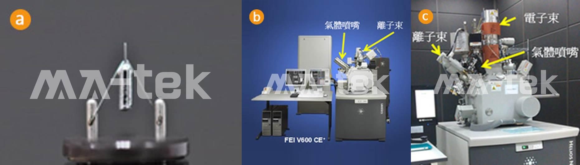
- Liquid metal ion source.
- Single beam system, equipped with various reaction gases such as: Br2、XeF2TEOS, specialized for circuit editing.
- Dual beam system, integrating electron beam and ion beam in one machine, specializing in precise location cross-section cutting and TEM sample preparation.
During the development phase of integrated circuit products, when the first batch of chips is produced, if there are design errors or malfunctions in the circuit, circuit modifications are needed to verify the circuit design. In the early days, modifying masks and re-taping for circuit modifications and verification was quite time-consuming and costly, especially as the integrated circuit process continued to miniaturize, the costs associated with this approach increased dramatically. Therefore, when FIB was able to perform deposition and etching of metal and insulating layers, it became a backend production line for miniaturized wafer fabs, capable of quickly providing circuit editing or mask repairs at a very low cost, thus accelerating product verification; at most, only one mask revision is needed to complete product development. Depending on the packaging of integrated circuit products and the specific locations that need editing, circuit editing can be divided into two main categories: front-side editing and back-side editing.
-
Front Editing
It starts from the top layer of the integrated circuit to the editing position of the lower metal layer, which means that it is necessary to dig through the protective layer and the upper metal wire layer to reach the desired editing position. The following Figure 2 is an example of the steps for front circuit editing. -
Backside editing
Construction starts from the bottom of the silicon wafer to the modification position, which means that it is necessary to drill through the silicon substrate and/or the underlying metal wire layer to the desired modification position. Figure 3 is an example of backside circuit modification.
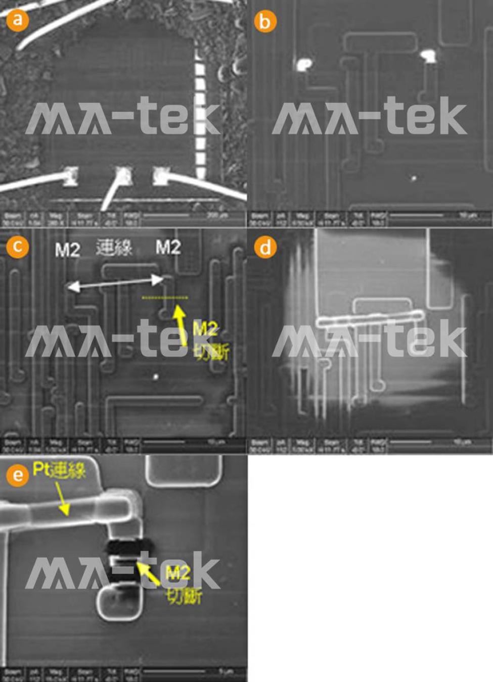
Generally speaking, the difficulty of editing varies depending on the differences in circuit structure. The larger the available excavation space at the construction editing location, the lower the construction difficulty; editing the upper metal wires is easier than editing the lower metal wires; aluminum metal wires are easier to work with than copper wires; front editing is easier than back editing. Common editing projects include:
- Excavation of the deep well of the insulation layer
- Cutting or piercing of metal wires
- Metal filling of the insulation layer deep well
- Metal connections, metal pads for bumping.
- Capacitor and resistor manufacturing
The deposition of the insulating layer is facilitated by the ion beam to promote the reaction gas decomposition, thereby generating SiO.2. Commonly used gases are TEOS or TMCTS. For metal deposition, the reaction gas for platinum (Pt) deposition is (CH3)Pt(CpCH3), deposition of tungsten (W) W(CO)6 。
FIB deposition of W has a lower resistivity than Pt, and its ability to fill holes is better, but the deposition rate is relatively slow, requiring a longer construction time. The deposition gas for carbon films is C10H8, and aluminum metal etching can use iodine (I.2)、Bromine (Br2)or chlorine (Cl2to achieve. The etching of copper uses gallium and moisture to sputter copper metal; the etching of the insulating layer uses XeF.2to achieve chemical etching reactions.
(a) IC Decapsulation
(b) Openings and Filling Metals
(c) Connection and Disconnection (Plan)
(d) Pt connection
(e) M2 Cut-off (Results after completion)
FIB can precisely excavate at the location where cross-sectional cutting is needed. Failure analysis or process monitoring often uses dual-beam FIB for specific point observation. First, an electron beam image (i.e., SEM image) is used to search for the cutting position, and after locating it, FIB is used for cutting. After the cross-section is completed, an electron beam is used to obtain the image of the cross-section, as shown in Figure 4(a). Figure 5(b) shows the cross-sectional structure of an integrated circuit in the copper wire process.
-
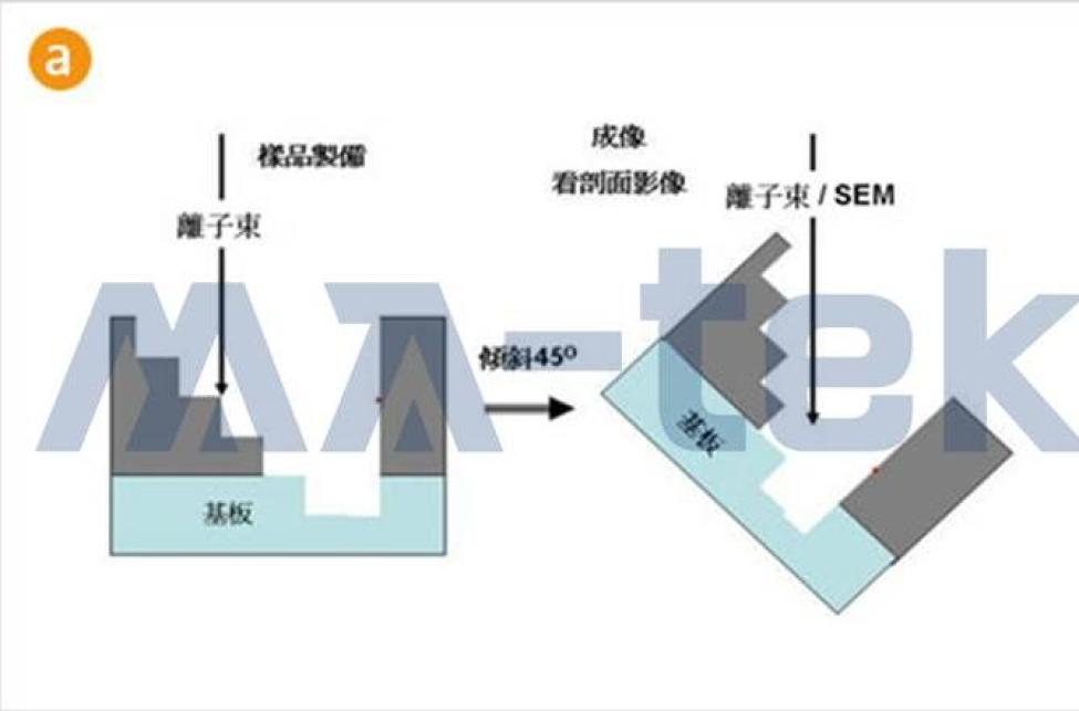
Figure | (a) Schematic diagram of the process for preparing cross-sectional samples using FIB.
-
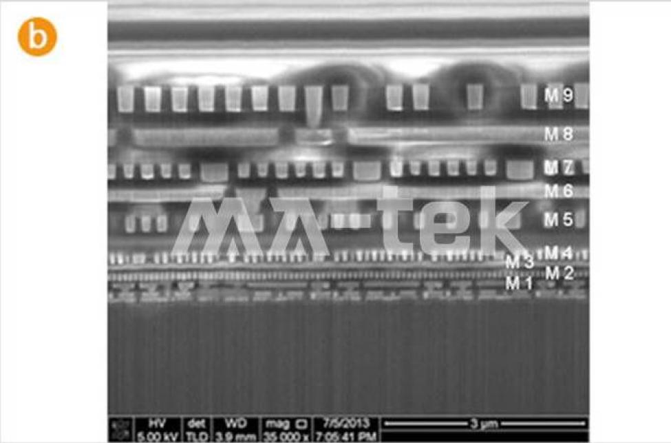
Figure | (b) Cross-sectional SEM image of the IC with 9 layers of metal processing after FIB point cross-section cutting.
When observing solid crystal samples, due to the regular arrangement of atoms, many regular lattice gaps similar to long channels are formed between specific crystal directions and crystal planes. When the ion beam is aligned with these directions, the ions can penetrate deeply without colliding with the surface atoms in the sample, resulting in no secondary electrons or backscattered incident ions being produced, thus the signals received by the signal detector are weaker.
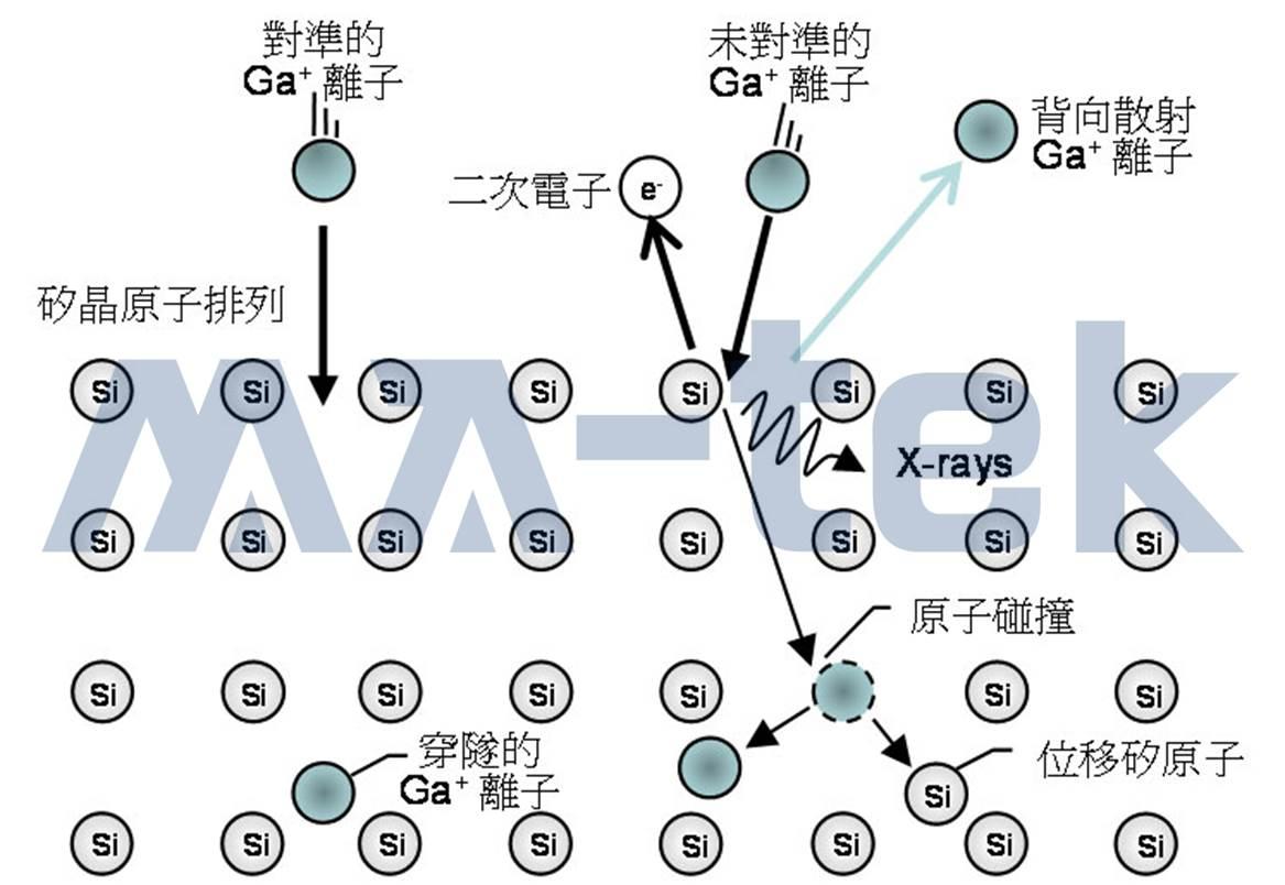
When observing solid crystal samples, due to the regular arrangement of atoms, many regular lattice gaps similar to long channels are formed between specific crystal directions and crystal planes. When the ion beam is aligned with these directions, ions can penetrate directly without colliding with the surface atoms in the sample, resulting in no secondary electrons or backscattered incident ions being generated, thus the signal received by the signal detector is weaker.
However, if the ion beam is not aligned with these directions, it will collide with the sample atoms at the surface, resulting in a greater number of secondary electrons or backscattered incident ions being generated, leading to a stronger signal received by the signal detector. Therefore, the obtained image will have a significant contrast in brightness, which is known as the ion channel contrast effect, as shown in Figure 6.
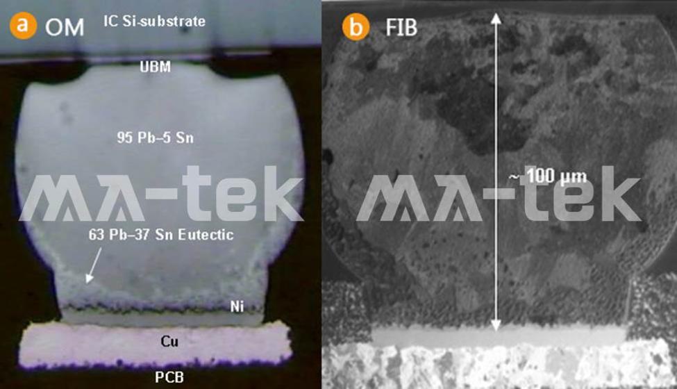
For the preparation of TEM samples in FIB cross-section, there are three methods: Pre-Thin, Lift-out, and Omni-probe. The choice of FIB depends on the analysis requirements of the sample.
pre-thinning method
Figure 8(a) and (b) show the preparation of samples using the pre-thinning method. The samples are first thinned to 5-10 um by grinding, and then further thinned to a thickness of 0.1 um suitable for TEM observation using FIB. The advantage of this method is that it can produce very large area (~50 um) and uniformly thick TEM samples; since the thin area is still held by the same material around it, there is no concern about deformation or curling of the thin area sample. However, this method requires grinding and then FIB cutting, making it more labor-intensive and time-consuming, and there is still a risk of failure during grinding.
-
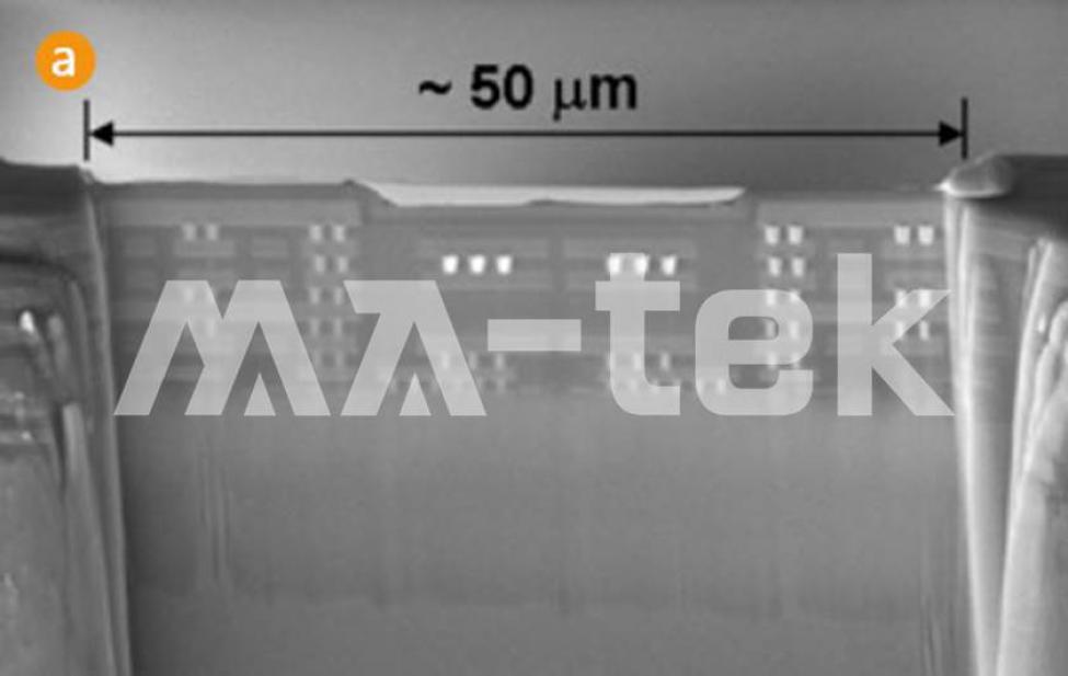
Figure | (a) Pre-Thin
-
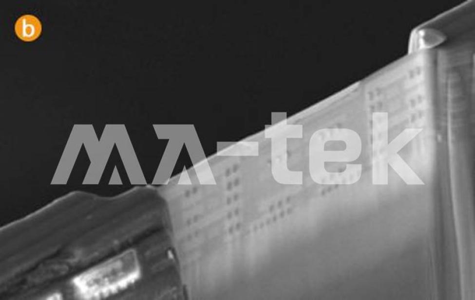
Figure | (b) Pre-Thin method
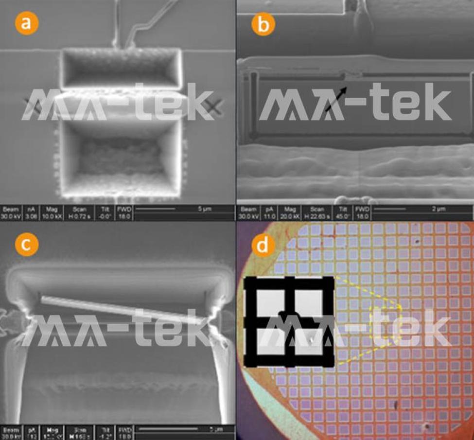
Electrostatic suction method
Figure 9 shows the preparation of samples using the suction method. First, the sampling area is thinned using FIB, then the thin sheet is separated from the sample using U-shaped cutting, and finally, it is extracted with a glass probe using electrostatic adsorption and placed on a copper grid with a carbon film. This is currently the fastest and most time-saving method for preparing TEM samples, with each sample taking less than 1 hour to produce. Therefore, this method is used for the mass production of TEM samples. However, once these samples are placed on the carbon film, no further processing or rework can be done, which means that the optimal quality of the samples cannot be guaranteed. Ultimately, the judgment of the final sample thickness still relies on the work experience of the FIB engineer.
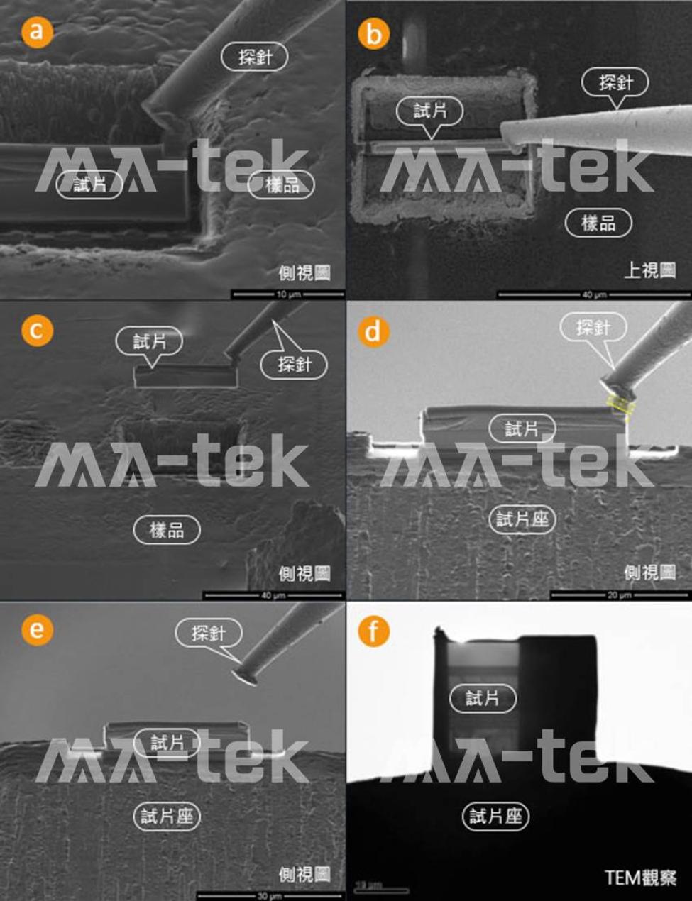
Probe extraction method
Figure 10 shows the probe extraction method, where the sample is roughly cut to about 1-2 mm using FIB to detach it from the specimen. Then, Pt is deposited using FIB to weld the probe to the specimen, and the probe is moved to transfer the specimen to the specimen holder. After welding the specimen to the specimen holder with Pt deposited by FIB, the probe is cut away from the specimen using FIB, and finally, the specimen is finely trimmed to a thickness suitable for TEM observation using FIB.
This is the most complex and time-consuming method for preparing TEM samples, with a total working time of approximately 1.5 to 2 hours. However, this method allows for repeated entry and exit from the FIB for further processing if any adjustments to the sample thickness are needed after TEM observation. Therefore, it ensures zero errors and zero risks in TEM sample preparation, and this method is usually adopted for very important sample analyses.
Left image 10 records the steps of the probe extraction method (Omni-probe) for TEM sample preparation:
(a), (b) Attach the probe to the cut specimen.
(c) Probe extraction
(d) Attach the sample to the sample holder.
(e) Cut the probe on the sample.
(f) Place the specimen holder and specimen into the TEM for observation.


