
AES OJ Electronics Energy Spectrum Analyzer
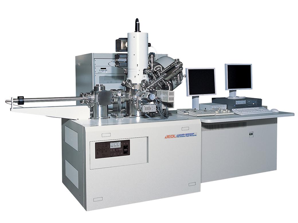
Field Emission Auger Electron Spectroscopy (JAMP-9500F)
It can provide high-resolution surface elemental analysis capabilities at the nanoscale. The system combines a high-resolution scanning electron microscope (SEM) with Auger electron spectroscopy technology, allowing for simultaneous observation of surface morphology and elemental analysis.
JAMP-9500F uses a hemispherical energy analyzer and a high-brightness field emission gun, providing high energy resolution and excellent spatial resolution. This equipment is particularly suitable for nanoscaleSurface element analysis, contamination analysis, and thin film interface research:
-
The resolution of SEM images can reach approximately 3 nm.
-
Auger Mapping resolution can reach approximately 8 nm.
Common applications include:Surface contamination and residue analysis,Analysis of element distribution in thin films and multilayer structures,Surface oxide layer and interface analysis,Nano-scale element mapping,Semiconductor process and material failure analysis,Through high-resolution surface analysis capabilities, FE-AES can provide material surface approximately5–8 nm depth rangethe elements and chemical information, is an important tool for analyzing nanometer-scale materials and microelectronic components.
-
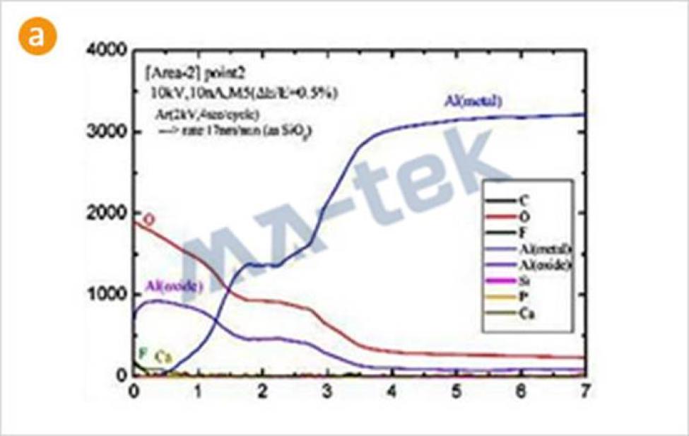
(a) Al pad depth profiling spectroscopy
-
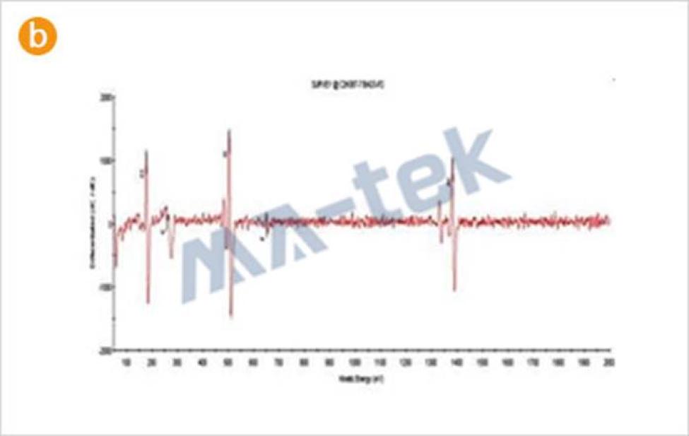
(b) Al pad surface analysis spectroscopy
-
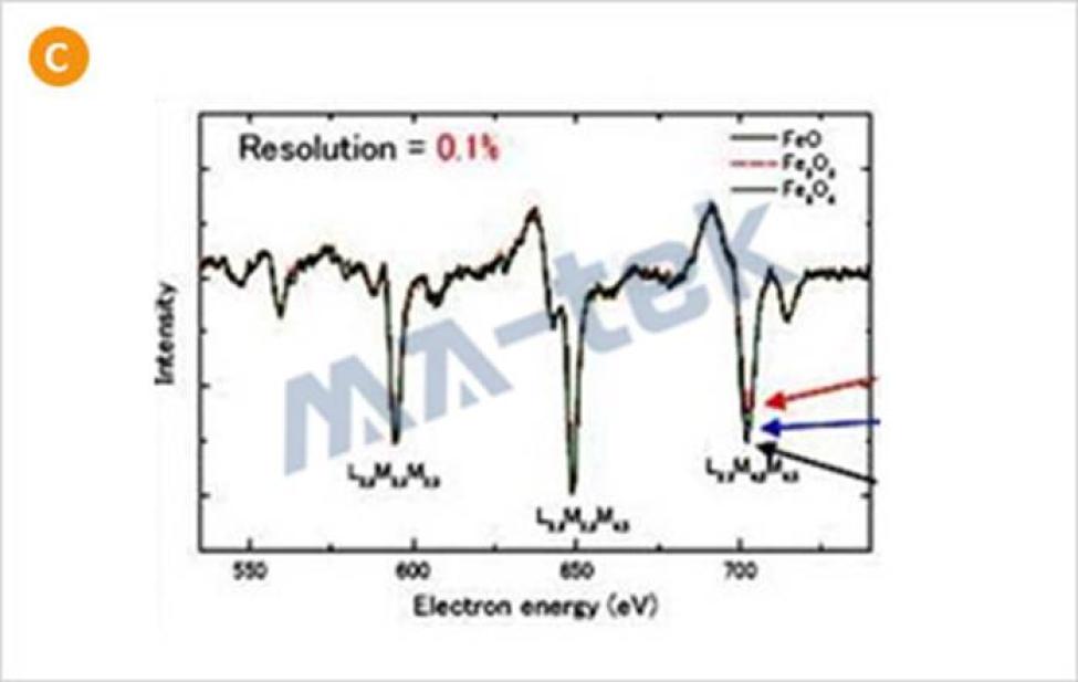
(c) Chemical state analysis of iron oxide
-
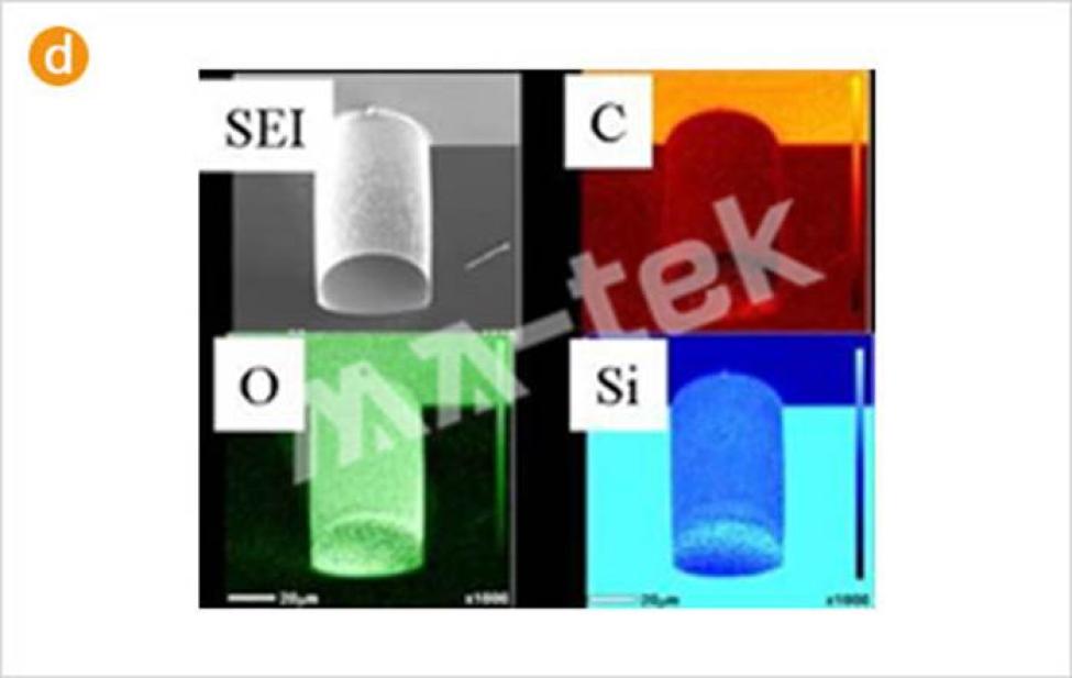
(d) Through-silicon vias (TSV) AES mapping


