
MA-tek focuses on the world's most advanced semiconductor testing technology and investment layout.
The world's top ultra-atomic resolution electron microscope is activated to support the research and production of processes below 2nm.
Leveraging industry-leading advanced process and packaging analysis technology, MA-tek has long provided global semiconductor leaders with GAAFET (Gate-all-around Field-Effect Transistor) structure inspection and advanced packaging failure analysis solutions such as CoWoS (Chip on Wafer on Substrate) and InFO (Integrated Fan-Out). To assist wafer manufacturers in advancing the research and development and mass production of processes below 2nm, MA-tek has invested in a world-class ultra-high resolution spherical aberration corrected transmission electron microscope (Cs Corrector TEM) at the Hsinchu Science Park.
The total investment in the equipment exceeds 5 million USD, with a height of up to 3.3 meters, and the purchase price is more than three times that of traditional electron microscopes. Its excellent imaging performance can accurately analyze dumbbell-shaped symmetrical images below 1nm, presenting details of atomic arrangements at the sub-angstrom level, providing unprecedented analytical capabilities for the research of materials and structures in processes below 2nm, accelerating semiconductor technology innovation. The equipment has been installed and officially put into service today (2025/4/1).
MA-tek has long been committed to research and development in cutting-edge technology, accumulating several years of experience in ultra-atomic detection and analysis. In 2019, another ultra-high resolution atomic resolution transmission electron microscope (Neo ARM, atomic resolution microscope) was installed in the laboratory in Nagoya, Japan. It is not only equipped with spherical aberration correction and provides ultra-high resolution images, but also has EELS functionality, which can better meet the detection needs of customers, adding more analytical capabilities to the structural analysis laboratory for use by Toyota Motor Corporation and Denso Research Center.
-
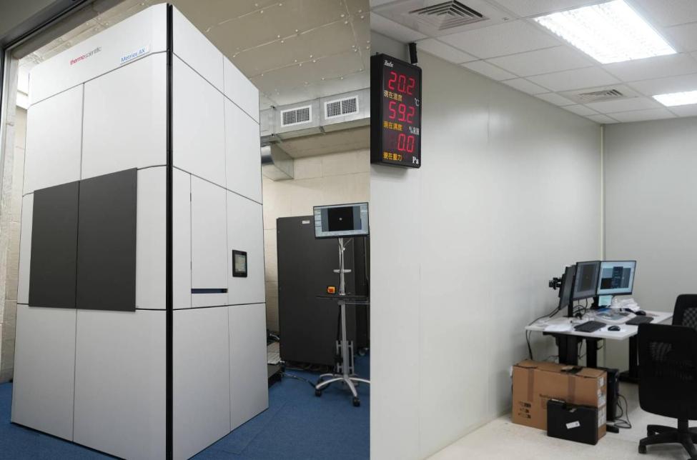
Spherical Aberration Corrected Transmission Electron Microscope (ThermoFisher Metrios AX TEM)
-
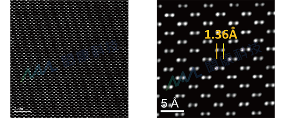
The imaging results of the dumbbell-shaped symmetrical arrangement of silicon materials at the ultra-angstrom level. 1 micron (μm) = 1000 nanometers (nm) = 10000 angstroms (Å)
the world's first nano-scale quantum device 3D imaging analysis technology
In recent years, MA-tek has collaborated with Professor Li Pei-wen from National Yang Ming Chiao Tung University to engage in industry-academia cooperation for the manufacturing and synthesis of quantum devices. Utilizing the 3D imaging technology of the microscope, they successfully established the world's first three-dimensional images of quantum dot devices. The 3D imaging technology provides atomic-level structural information of quantum dot devices in quantum computing and silicon photonics applications, accurately analyzing the geometric morphology, diameter, and crystal orientation of quantum dots, thereby advancing the research progress of qubits, quantum sensing technology, and silicon photonic devices. This groundbreaking tool not only achieves high sensitivity detection but also enables precise three-dimensional structural analysis, laying the foundation for the development of quantum computing and silicon photonic technology. Figures 1 and 2 illustrate the 3D imaging construction technology of germanium quantum dot (Quantum Dots, QDs) devices.
-
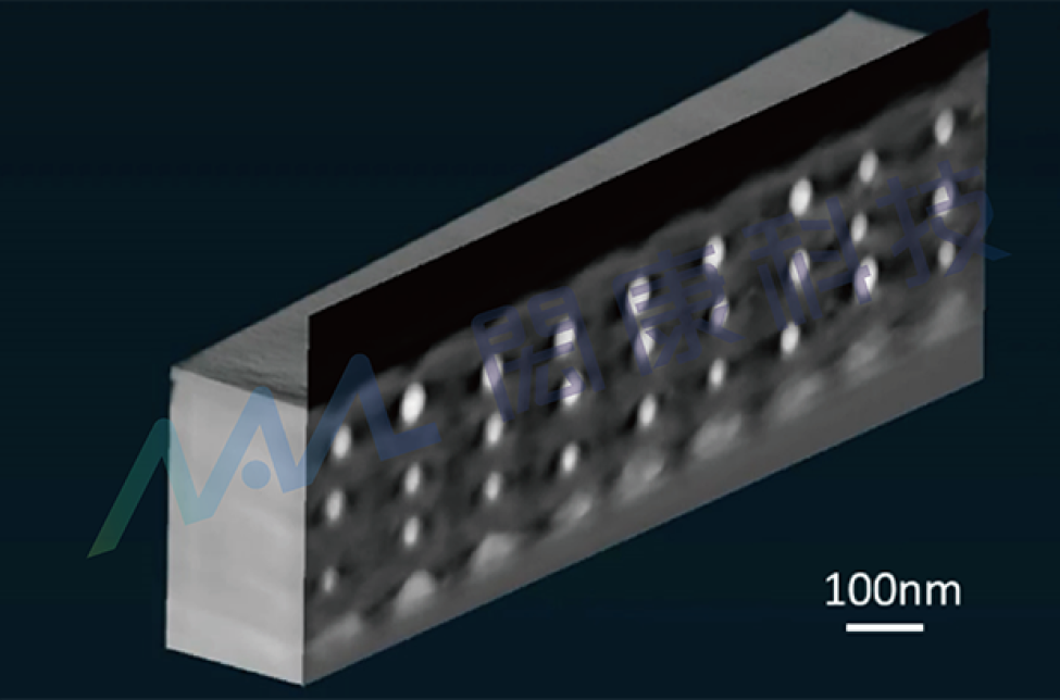
Figure 1 shows the overall specimen after 3D reconstruction, allowing inspection of any cross-sectional slice structure within the volume. The white dot-like objects are germanium quantum dots.
-
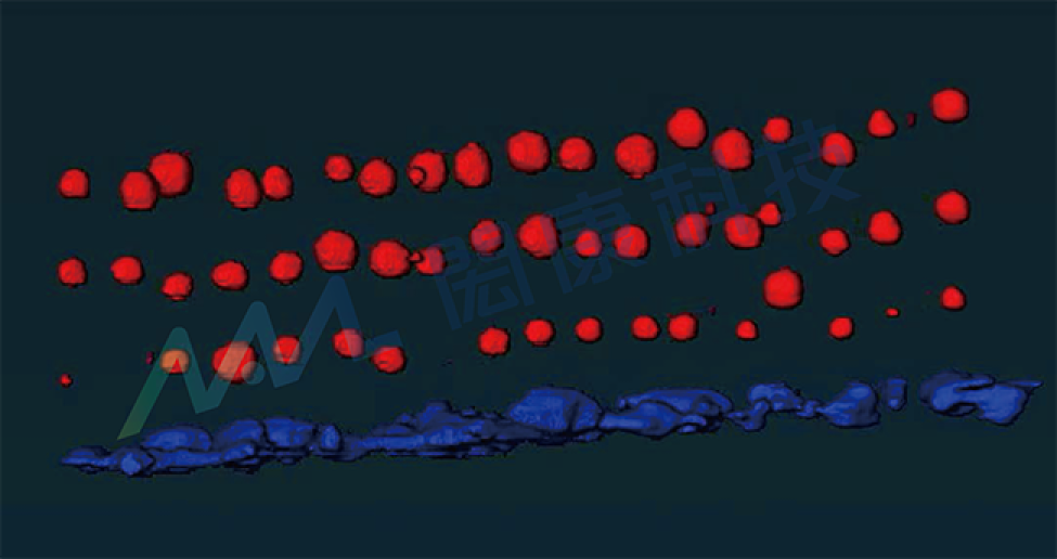
Figure 2. The red area represents germanium quantum dots, allowing the entire sample to be rotated 360 degrees to observe the overall arrangement of the QDs.
Expand investment in ultra-high power reliability verification equipment to meet the demand of the AI chip market.
To meet the reliability testing needs of high-end AI chips, MA-tek completed the installation of 2 Incal/Sonoma machines and 2 MCC/HPB6 machines in the first quarter of 2025, with the capability to verify power of up to 800 watts and 1500 watts per single IC, leading globally in laboratory technology. The equipment has received validation projects from top autonomous vehicle and AI chip manufacturers in Europe and the United States, covering single device, board-level, and module testing, providing critical reliability verification services for the global AI market.
This investment will further strengthen MA-tek's technological advantages in the field of AI chip reliability verification, and is expected to bring significant revenue growth starting from the fourth quarter of 2025, continuing to consolidate its competitive edge in the semiconductor testing and analysis market.
-
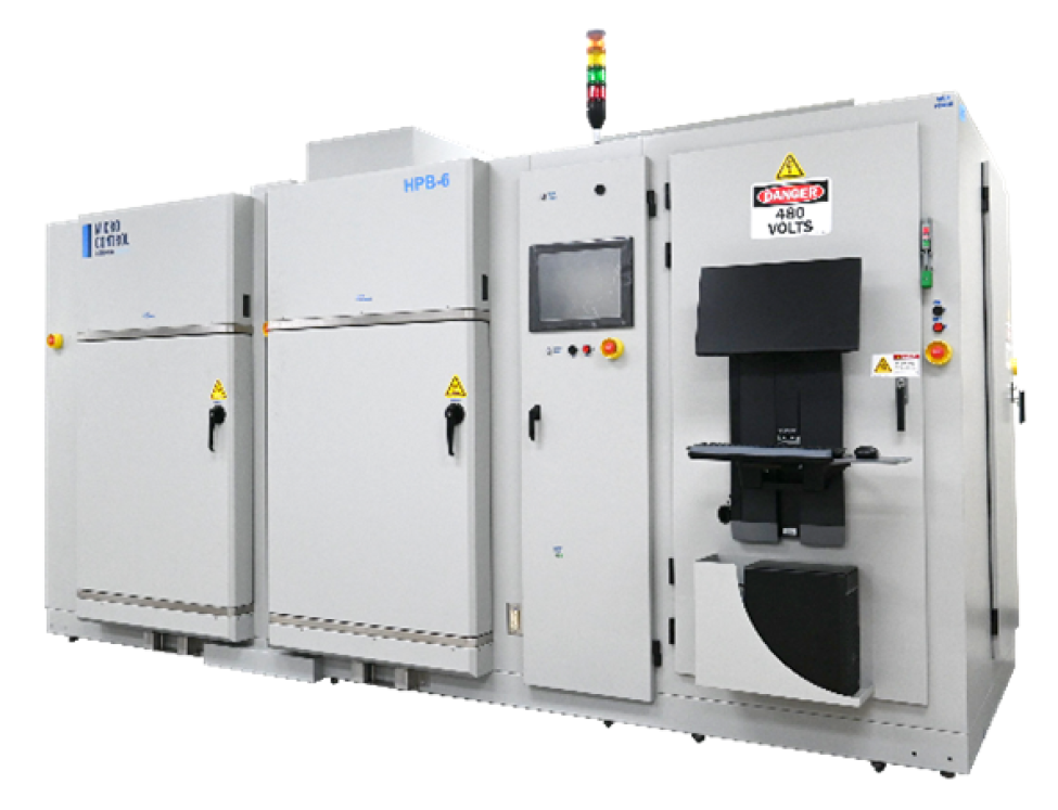
MCC HPB6 ultra-high power pre-burner (1500W)
-
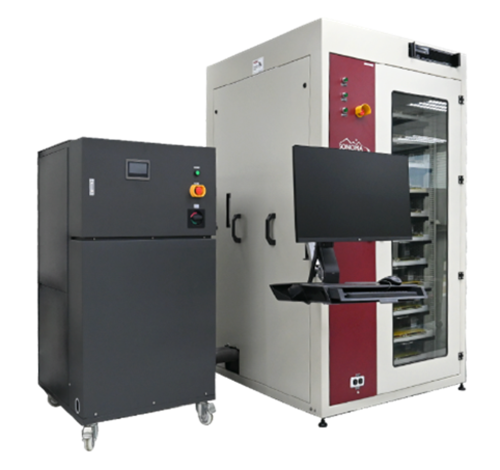
Incal Sonoma ultra-high power pre-burner (800W)
Looking to the future, actively expanding the global market territory.
As semiconductor technology continues to evolve, MA-tek will continue to increase investment in technology research and development and equipment, deepen cooperation with the global semiconductor supply chain, and actively expand into international markets. With continuous innovative breakthroughs and technological leadership advantages, MA-tek will continue to provide the most advanced and precise semiconductor analysis and testing services to global customers, further consolidating its market leadership position.
News Links
-
[Liberty Times] MA-tek makes a significant investment in equipment, securing orders for American self-driving cars.
- 【United News Network] Taiwan's first top-tier TEM goes into service, accelerating R&D and verification below 2nm.
- 【MoneyDJ News】MA-tek's revenue in Japan is expected to double in 2025, with strong operational performance throughout the year.


